Silicon carbide semiconductor device and method for manufacturing the same

Active Publication Date: 2015-02-19
DENSO CORP +1
View PDF3 Cites 19 Cited by
  • Summary
  • Abstract
  • Description
  • Claims
  • Application Information

AI Technical Summary

Benefits of technology

[0009]In view of the above circumstances, the present disclosure aims at providing an SiC semiconductor device with a structure that can further rest

Problems solved by technology

Therefore, the switching characteristic is deteriorated.
The electric field is concentrated on the gate insulating f

Method used


Image

  • Silicon carbide semiconductor device and method for manufacturing the same
  • Silicon carbide semiconductor device and method for manufacturing the same
  • Silicon carbide semiconductor device and method for manufacturing the same

Examples


first embodiment

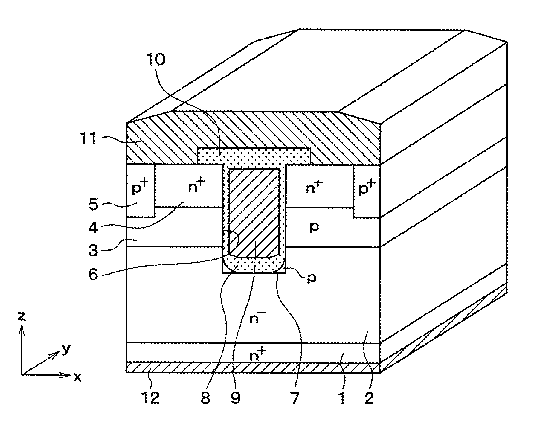
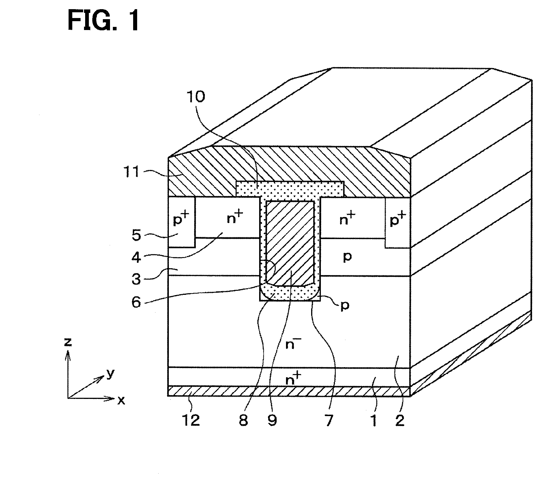
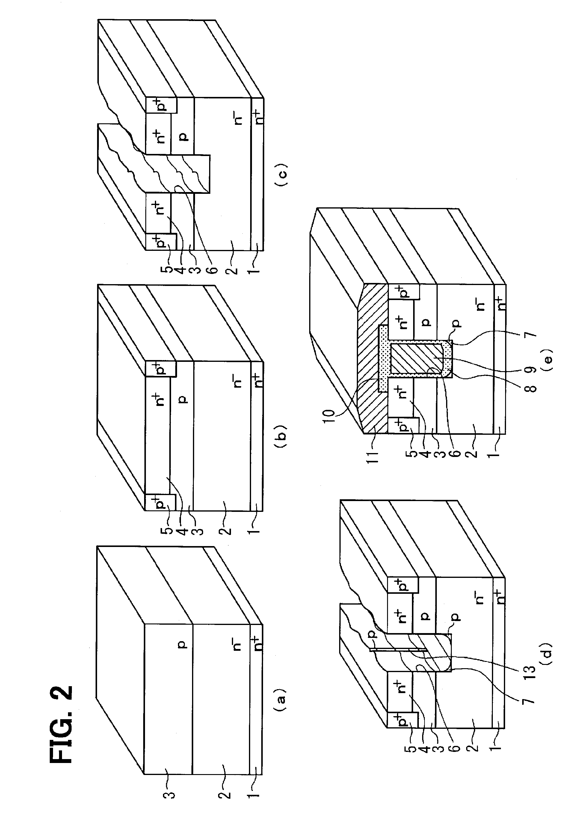
[0022]A first embodiment of the present disclosure will be described. In the description, a semiconductor switching element having a trench gate structure will be exemplified by an SiC semiconductor device in which an inversion type MOSFET is formed.

[0023]As illustrated in FIG. 1, an inversion type MOSFET of an n-channel type is formed in the SiC semiconductor device. MOSFETs having the same structure as that of the MOSFET illustrated in the figure are arranged in plural rows adjacent to each other to configure the MOSFETs of plural cells. Specifically, a semiconductor substrate is formed of an n+ type substrate 1 made of SiC, and the respective components of the MOSFET is formed over the n+ type substrate 1 to configure the MOSFET.

[0024]The n+ type substrate 1 is, for example, 1.0×10¹⁹ / cm3 in n-type impurity concentration such as nitrogen, and about 300 μm in thickness. An n− type drift layer 2 made of SiC which is, for example, 3.0×10¹⁵ to 2.0×10¹⁶ / cm3 in n-type impurity concentra...

second embodiment

[0057]A second embodiment of the present disclosure will be described. In the present embodiment, the shape of the trench 6 in the first embodiment is changed. Other configurations are similar to those in the first embodiment, and therefore only parts different from those in the first embodiment will be described.

[0058]As illustrated in FIG. 3, in the present embodiment, the trench 6 is formed into a triangular shape, that is, the bottom is formed into not a flat surface but a pointed taper shape. The p-type SiC layer 7 that is formed into a triangular round shape (triangular shape having a rounded side) in a cross section is formed in the corner of the bottom of the trench 6, such as in the tip end portion of the trench 6 in the case of the present embodiment. Even with the above structure, the existence of the p-type SiC layer 7 formed in the corner of the bottom of the trench 6 enables the electric field concentration on the bottom of the trench to be reduced when the MOSFET is o...


PUM


Abstract

In a silicon carbide semiconductor device, a p-type SiC layer is disposed in a corner of a bottom of a trench. Thus, even if an electric field is applied between a drain and a gate when a MOSFET is turned off, a depletion layer in a pn junction between the p-type SiC layer and an n type drift layer greatly extends toward the n type drift layer, and a high voltage caused by an influence of a drain voltage hardly enters a gate insulating film. Hence, an electric field concentration within the gate insulating film can be reduced, and the gate insulating film can be restricted from being broken. In this case, although the p-type SiC layer may be in a floating state, the p-type SiC layer is formed in only the corner of the bottom of the trench. Thus, the deterioration of the switching characteristic is relatively low.

Description

CROSS-REFERENCE TO RELATED APPLICATIONS[0001]The present disclosure is a U.S. national stage application of International Patent Application No. PCT / JP2013 / 002594 filed on Apr. 17, 2013 and is based on Japanese Patent Application No. 2012-95517 filed on Apr. 19, 2012, the contents of which are incorporated herein by reference.TECHNICAL FIELD[0002]The present disclosure relates to a silicon carbide (hereinafter referred to as “SiC”) semiconductor device having a semiconductor switching element with a trench gate structure, and a method of manufacturing the same.BACKGROUND[0003]In the semiconductor device having the semiconductor switching element, an increase in channel density is effective in allowing a larger current to flow. In a silicon transistor, in order to increase the channel density, a MOSFET having a trench gate structure is employed, and put into practical use. The trench gate structure can be also applied to an SiC semiconductor device. However, when the trench gate stru...

Claims


Application Information

Patent Timeline
IPC IPC(8): H01L29/423H01L29/10H01L21/265H01L29/66H01L21/3065H01L21/324H01L29/16H01L29/78
CPCH01L29/4236H01L29/1608H01L29/1095H01L29/7813H01L29/66068H01L21/3065H01L21/324H01L21/26513H01L29/66734H01L21/044H01L21/0465H01L29/0623H01L29/42368
Inventor TAKEUCHI, YUICHICHIDA, KAZUMISOEJIMA, NARUMASAWATANABE, YUKIHIKO
Owner DENSO CORP
Why Eureka
Try Eureka