Method for manufacturing electronic component embedding substrate and electronic component embedding substrate

Inactive Publication Date: 2015-02-19
SAMSUNG ELECTRO MECHANICS CO LTD
View PDF1 Cites 2 Cited by
  • Summary
  • Abstract
  • Description
  • Claims
  • Application Information

AI Technical Summary

Benefits of technology

[0010]An object of the present invention is to provide a method for manufacturing an electronic component embedding substrate and an electronic component embedding substrate that are capable of improving bonding force on a bonding interface by primarily stacking

Problems solved by technology

In the case of a low CTE (Coefficient of Thermal Expansion) resin, an amount of filler is further increased, such that bonding force of the resin is r

Method used


Image

  • Method for manufacturing electronic component embedding substrate and electronic component embedding substrate
  • Method for manufacturing electronic component embedding substrate and electronic component embedding substrate
  • Method for manufacturing electronic component embedding substrate and electronic component embedding substrate

Examples


Embodiment Construction

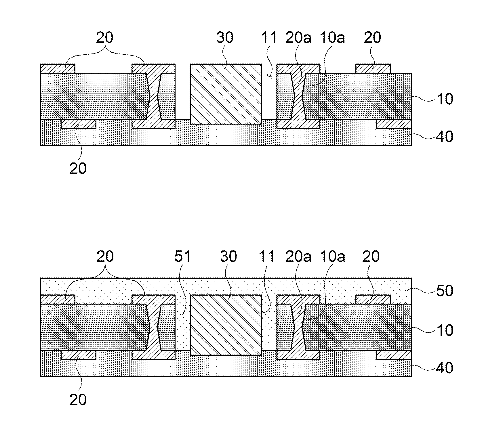
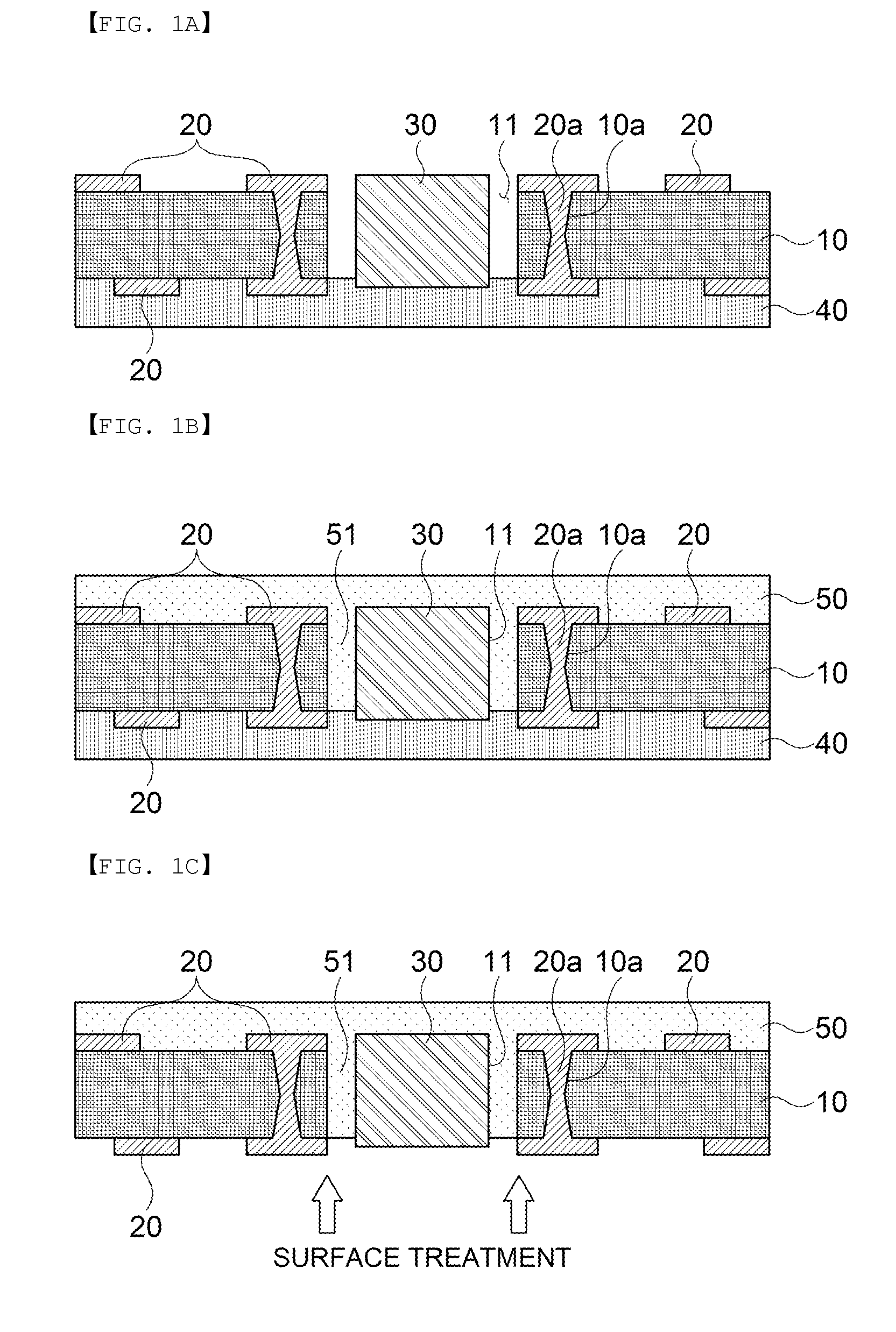
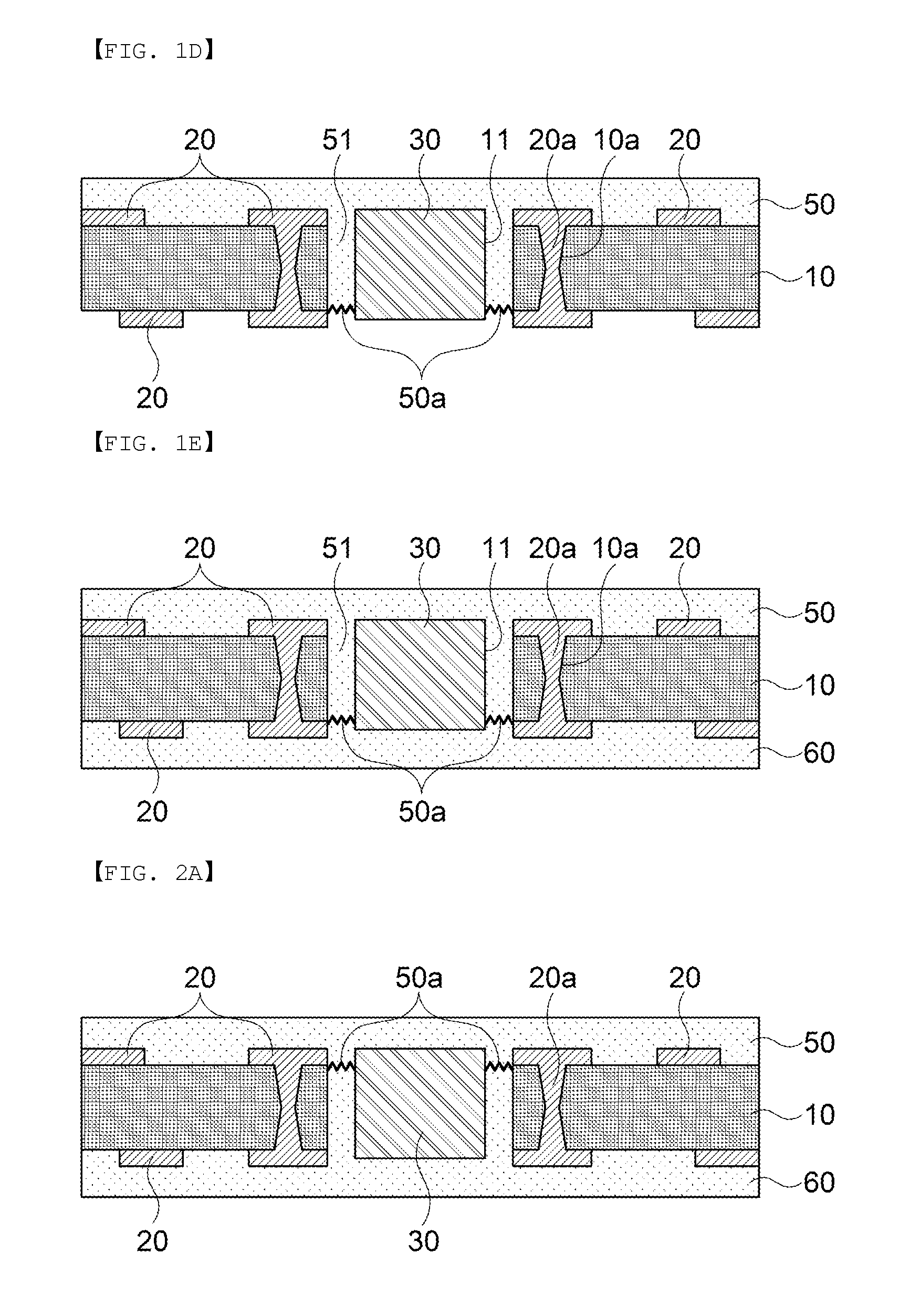
[0025]Exemplary embodiments of the present invention for accomplishing the above-mentioned objects will be described with reference to the accompanying drawings. In the description, the same reference numerals will be used to describe the same components of which a detailed description will be omitted in order to allow those skilled in the art to understand the present invention.

[0026]In the specification, it will be understood that unless a term such as ‘directly’ is not used in a connection, coupling, or disposition relationship between one component and another component, one component may be ‘directly connected to’, ‘directly coupled to’ or ‘directly disposed to’ another element or be connected to, coupled to, or disposed to another element, having the other element intervening therebetween.

[0027]Although a singular form is used in the present description, it may include a plural form as long as it is opposite to the concept of the present invention and is not contradictory in v...


PUM

PropertyMeasurementUnit
Interface roughnessaaaaaaaaaa
Surface roughnessaaaaaaaaaa
aaaaaaaaaa

Abstract

Disclosed herein are a method for manufacturing an electronic component embedding substrate and an electronic component embedding substrate. The method for manufacturing an electronic component embedding substrate includes: inserting an electronic component into a cavity formed in a core substrate; stacking a first insulating layer on one side of the core substrate into which the electronic component is inserted; performing surface treatment on the other side of the core substrate opposite to a direction in which the first insulating layer is stacked to improve a surface roughness of at least an exposed surface of the first insulating layer; and stacking a second insulating layer on the other side of the core substrate so as to be bonded to the exposed surface of the first insulating layer of which the surface roughness is improved. In addition, disclosed herein is the electronic component embedding substrate.

Description

CROSS REFERENCE(S) TO RELATED APPLICATIONS[0001]This application claims the foreign priority benefit under 35 U.S.C. Section 119 of Korean Patent Application Serial No. 10-2013-0096648, entitled “Method for Manufacturing Electronic Component Embedding Substrate and Electronic Component Embedding Substrate” filed on Aug. 14, 2013, which is hereby incorporated by reference in its entirety into this application.BACKGROUND OF THE INVENTION[0002]1. Technical Field[0003]The present invention relates to a method for manufacturing an electronic component embedding substrate and an electronic component embedding substrate.[0004]2. Description of the Related Art[0005]In accordance with development of an electronic industry, the demand for multi-functionalization and miniaturization of an electronic component has increased. Particularly, in accordance with thinness and lightness of a personal portable terminal, a printed circuit board tends to be thinned and become light, and an effort to prov...

Claims


Application Information

Patent Timeline
IPC IPC(8): H05K1/02H05K3/30H05K1/18
CPCH05K1/0271H05K1/185H05K2201/068H05K2201/10431H05K3/30H05K1/0373H05K3/0017H05K2203/0156H05K2203/1476H05K3/4602H05K2203/1469Y10T29/4913H05K3/46H05K1/0298H05K1/115
Inventor KIM, HONG WONLEE, SEOK KYULEE, TAE GONKANG, BYUNG HAKBYUN, JUNG SOOYU, YEON SEOPYOON, SANG MI
Owner SAMSUNG ELECTRO MECHANICS CO LTD
Why Eureka
Try Eureka