Rigid flexible PCB and method for manufacturing the same

Inactive Publication Date: 2015-03-05
SAMSUNG ELECTRO MECHANICS CO LTD
View PDF5 Cites 14 Cited by
  • Summary
  • Abstract
  • Description
  • Claims
  • Application Information

AI Technical Summary

Benefits of technology

[0011]An object of the present invention is to provide a rigid flexible PCB capable of improving deviations in the overall thickness of the b

Problems solved by technology

Accordingly, the design of the printed circuit board becomes more complicated, and highly densed and smaller circuits are increasingly required.
Thus, La

Method used


Image

  • Rigid flexible PCB and method for manufacturing the same
  • Rigid flexible PCB and method for manufacturing the same
  • Rigid flexible PCB and method for manufacturing the same

Examples


Embodiment Construction

[0018]Hereinafter, exemplary embodiments of the present invention will be described in detail with reference to the accompanying drawings.

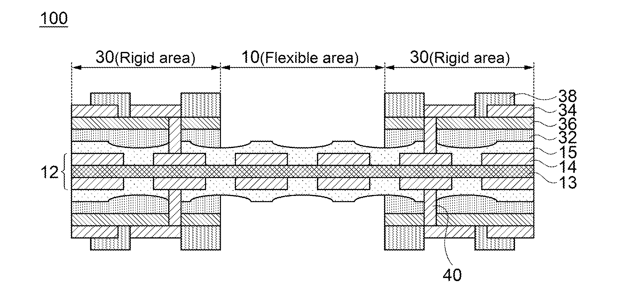
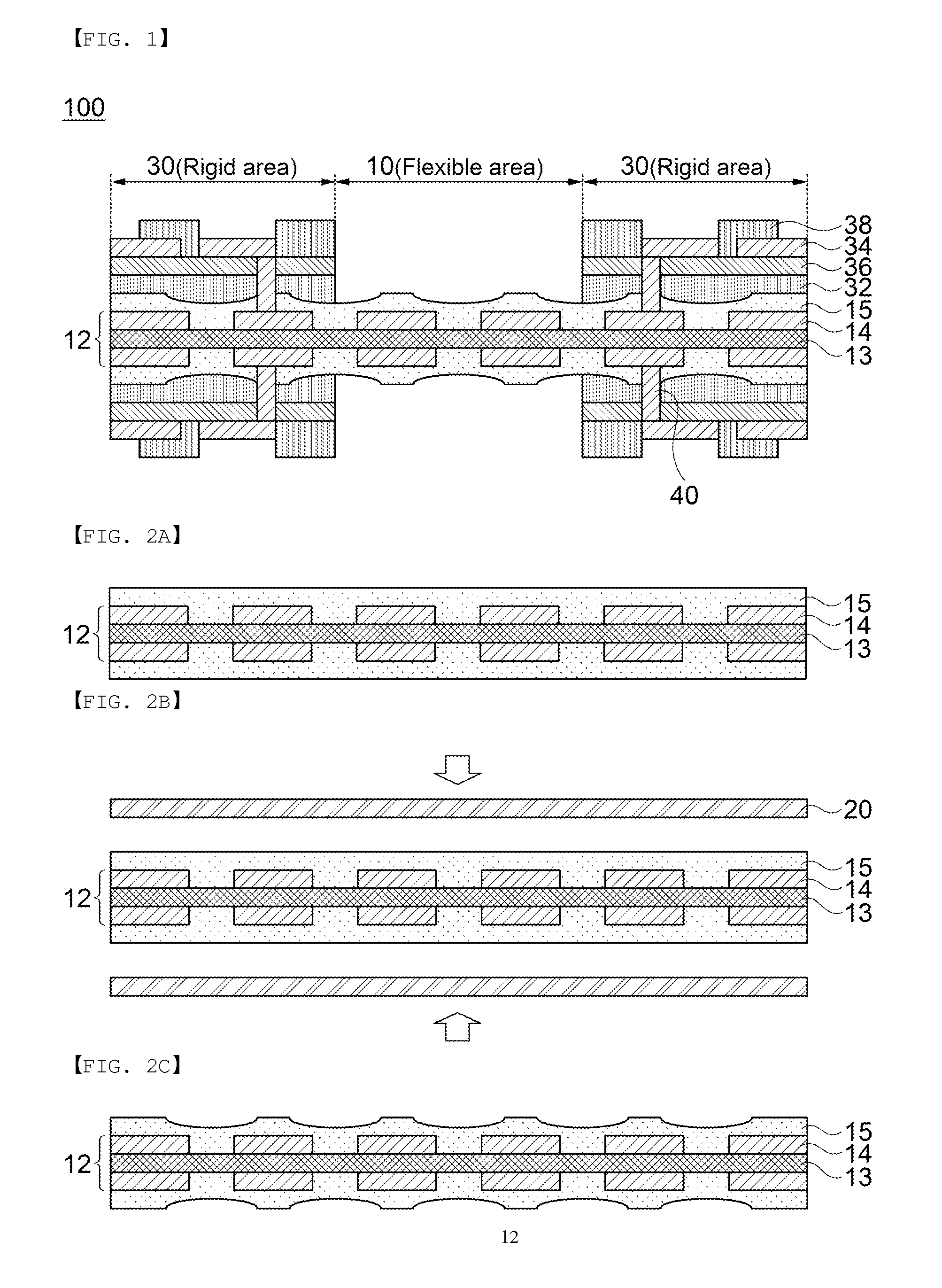
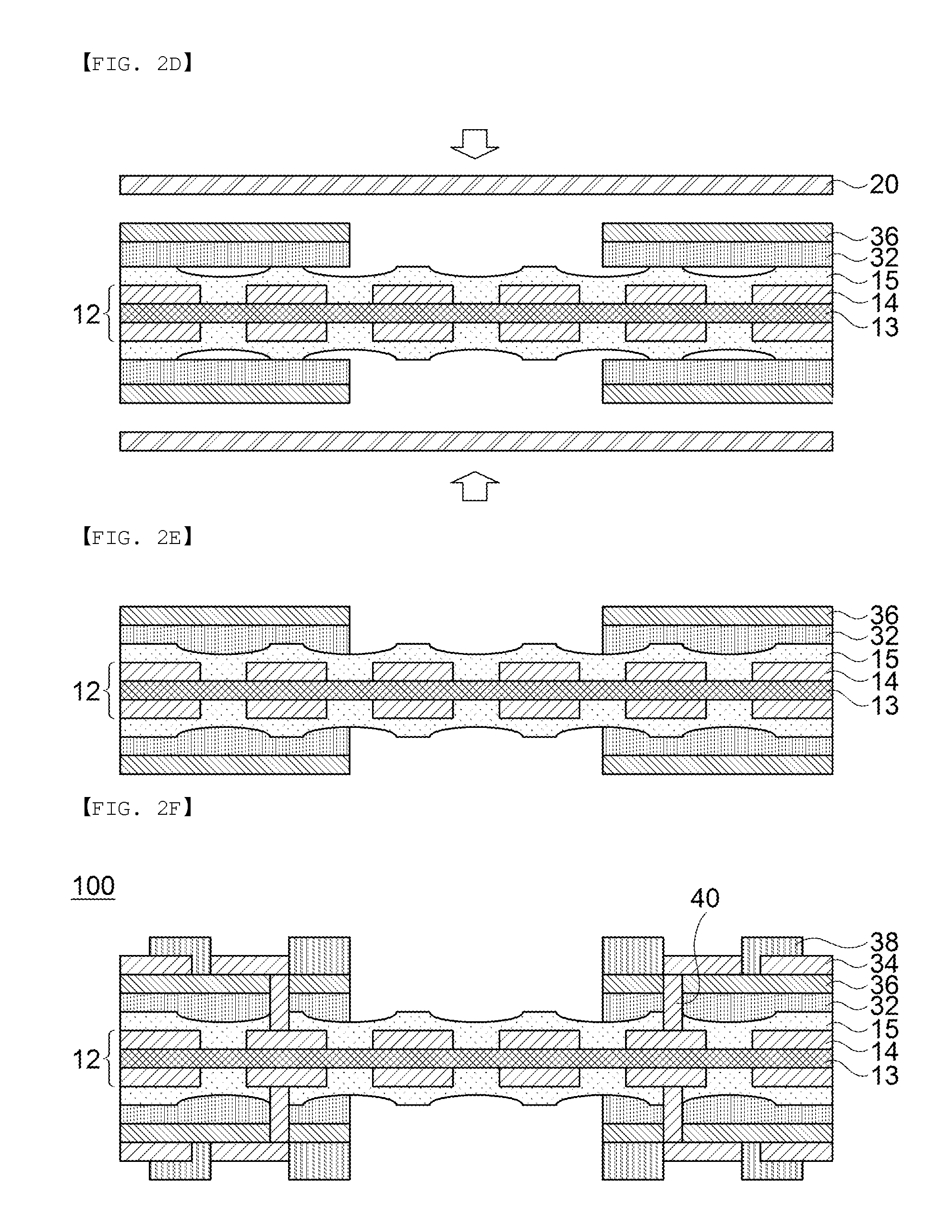
[0019]FIG. 1 is a cross-sectional view of a manufactured rigid flexible PCB according to an exemplary embodiment of the present invention; and FIGS. 2A to 2F are views showing a manufacturing process of the rigid flexible PCB according to an exemplary embodiment of the present invention.

[0020]As shown in FIG. 1, the rigid flexible PCB 100 according to the exemplary embodiment of the present invention includes a flexible area 10 and rigid areas 30 on both sides of the flexible area 10.

[0021]The flexible area 10 includes an insulating material 13 formed of polyimide or prepreg, a flexible copper foil laminate 12 having circuit layers 14 formed on both surfaces of the insulating material 13, and cover lays stacked on the flexible copper foil laminate 12.

[0022]Preferably, the insulating material 13 is thinner than or equal to the circuit layers 14. Th...


PUM

PropertyMeasurementUnit
Temperatureaaaaaaaaaa
Pressureaaaaaaaaaa

Abstract

Disclosed herein is a rigid flexible printed circuit board (PCB) including: a flexible area having a flexible copper foil laminate in which circuit layers are formed on an insulating material, and cover lays formed on the laminate; and rigid areas having insulating layers and copper layers built-up on both sides of the flexible area, and flattening materials to flatten outer surfaces of the insulating layers.

Description

CROSS REFERENCE(S) TO RELATED APPLICATIONS [0001]This application claims the benefit under 35 U.S.C. Section 119 of Korean Patent Application Serial No. 10-2013-0104834, entitled “Rigid Flexible PCB and Method for Manufacturing the Same” filed on Sep. 2, 2013, which is hereby incorporated by reference in its entirety into this application.BACKGROUND OF THE INVENTION [0002]1. Technical Field[0003]The present invention relates to a rigid flexible PCB and a method for manufacturing the same, and more particularly, to a rigid flexible PCB with improved flatness and a method for manufacturing the same.[0004]2. Description of the Related Art[0005]Recently, mobile electronic devices have evolved to have high performance and to support the Internet, video and massive data transmission. Accordingly, the design of the printed circuit board becomes more complicated, and highly densed and smaller circuits are increasingly required.[0006]Therefore, printed circuit boards incorporated in electron...

Claims


Application Information

Patent Timeline
IPC IPC(8): H05K3/46H05K1/09H05K1/11H05K1/02
CPCH05K3/4691H05K3/4673H05K1/028H05K2203/14H05K1/115H05K1/0298H05K1/09H05K3/4652Y10T29/302H05K1/02H05K3/46
Inventor PARK, JUNG YONGKO, TAE HOSONG, SEOK CHEOL
Owner SAMSUNG ELECTRO MECHANICS CO LTD
Why Eureka
Try Eureka