

Organic electroluminescence device
- Summary
- Abstract
- Description
- Claims
- Application Information
AI Technical Summary
Benefits of technology
Problems solved by technology
Method used
Image

Examples
examples 1 to 15
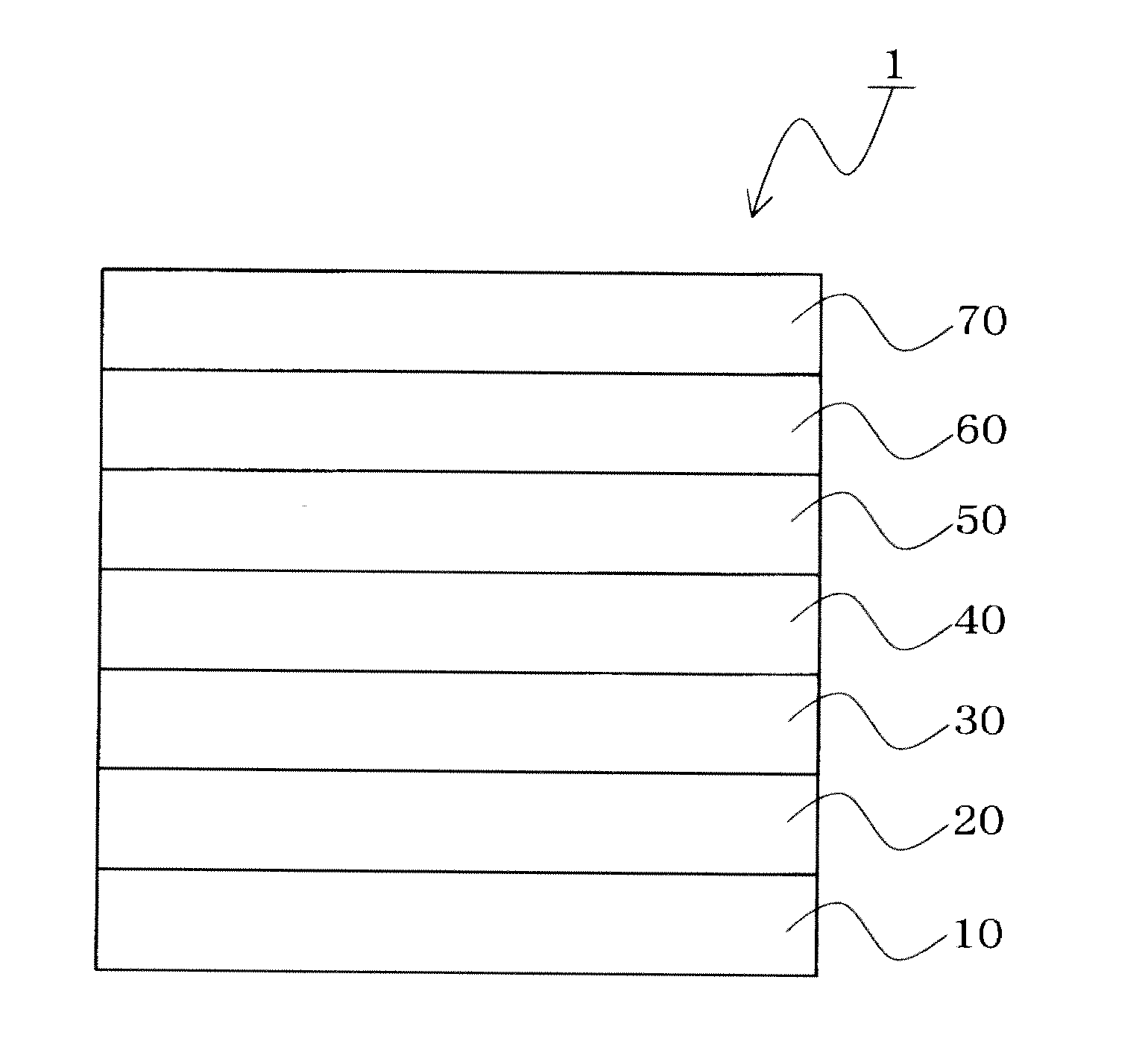
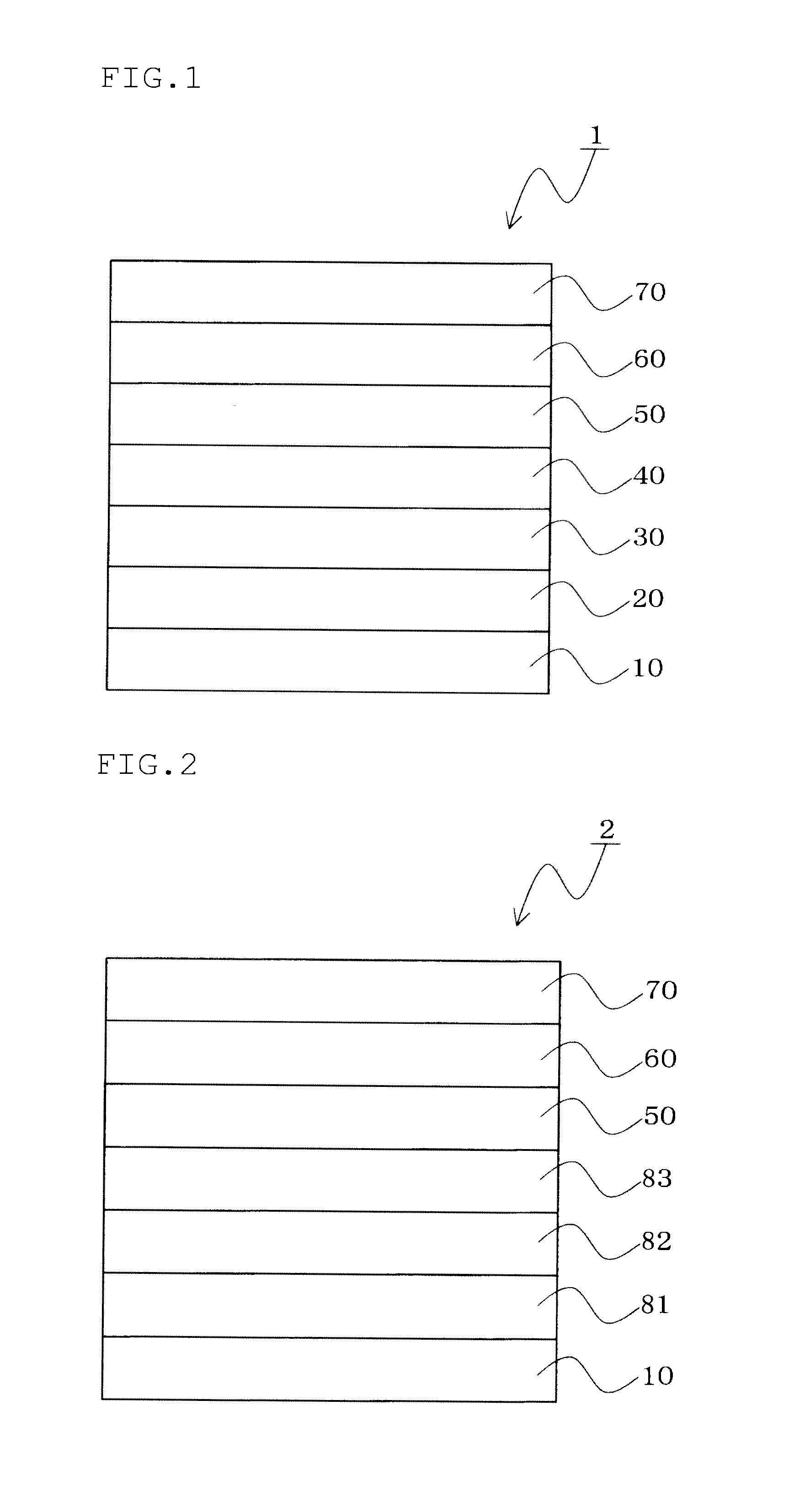
[0142]On a glass substrate having a dimension of 30 mm×30 mm, ITO was formed in a thickness of 240 nm as an anode. Subsequently, by deposition of SiO2, a cell for an organic EL device in which other parts than emitting regions of 2 mm×2 mm were masked by an insulating film was fabricated.
[0143]On the anode, as a hole-injecting layer, hexanitrileazatriphenylene ((HAT) represented by the following formula) was formed in a thickness of 10 nm.
[0144]On the hole-injecting layer, a hole-transporting layer, a blue-emitting layer and an electron-transporting layer were formed in this sequence.
[0145]Specifically, as the hole-transporting layer, the compound represented by the following formula (α-NPD) was formed into a 90 nm-thick film by the vacuum vapor deposition method (deposition speed: 0.2 to 0.4 nm / sec).
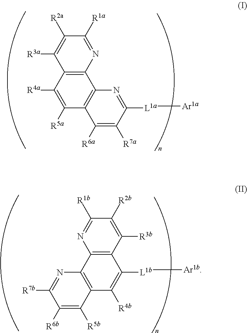
[0146]Subsequently, on the hole-transporting layer, the blue-emitting layer was formed. As the host for the emitting layer, the compound represented by the following formula (1) was use...
PUM
 Abstract
Description
Claims
Application Information