Semiconductor devices and fabrication methods thereof

a technology of semiconductor devices and semiconductors, applied in the direction of semiconductor devices, basic electric elements, electrical equipment, etc., can solve the problems of reducing the breakdown voltage, affecting the safety of the circuit, and the inability of the transistor to sustain a high voltage and a high current continuously

Active Publication Date: 2015-03-19
SEMICON MFG INT (SHANGHAI) CORP
View PDF1 Cites 11 Cited by
  • Summary
  • Abstract
  • Description
  • Claims
  • Application Information

AI Technical Summary

Problems solved by technology

Further, with the continuous shrinkage of the critical dimension of the CMOS processes, the ability of the transistors for sustaining a high voltage and a high current continuously decreases.
That is, a higher doping concentration of the drifting region may aid to reduce the on-resistance of a LDMOSFET or a LIGBT and to increase an on-current of the LDMOSFET or the LIGBT, but it may reduce the breakdown voltage of the LDMOSFET or the LIGBT, which may affect the safety of the circuit.

Method used


Image

  • Semiconductor devices and fabrication methods thereof
  • Semiconductor devices and fabrication methods thereof
  • Semiconductor devices and fabrication methods thereof

Examples


Embodiment Construction

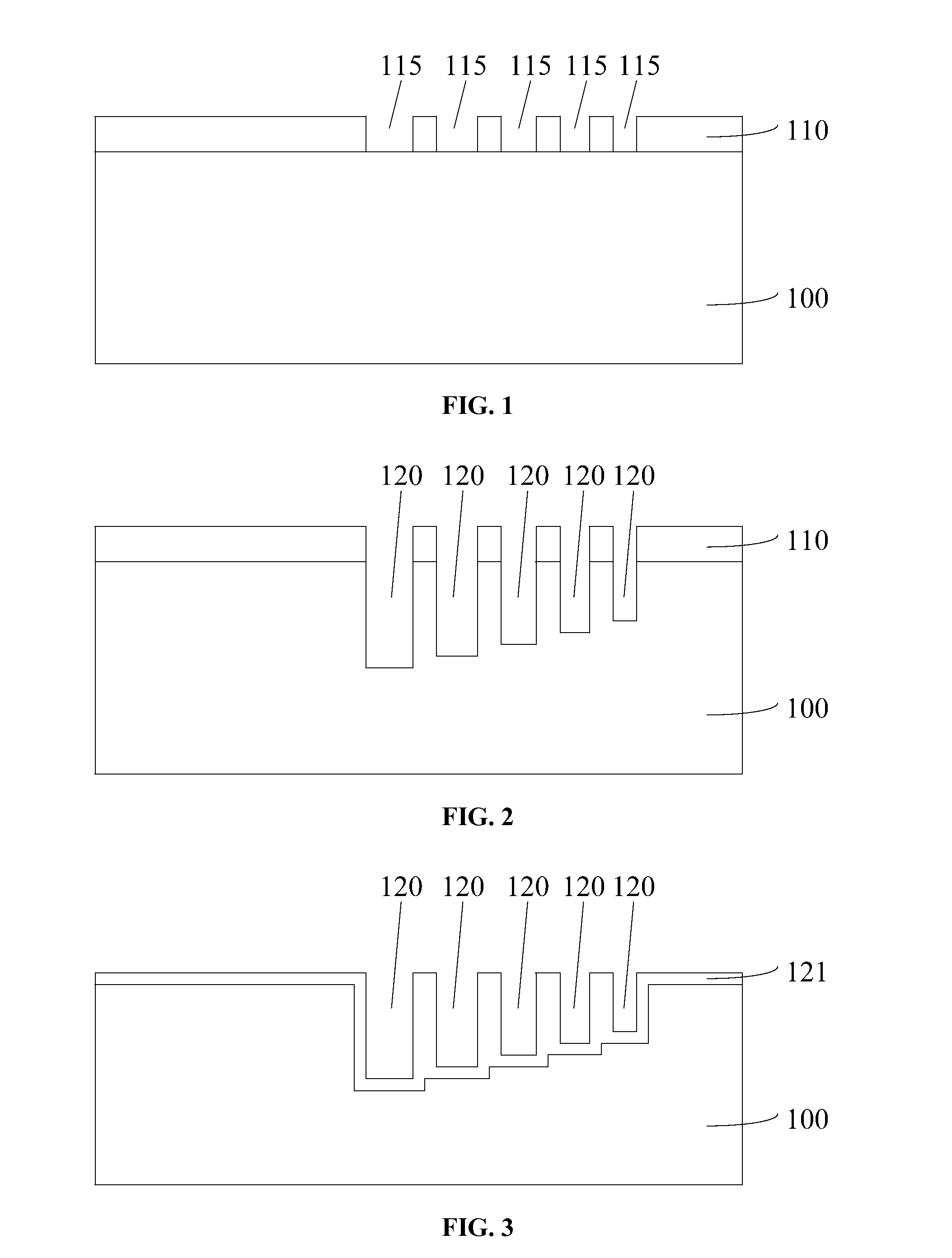
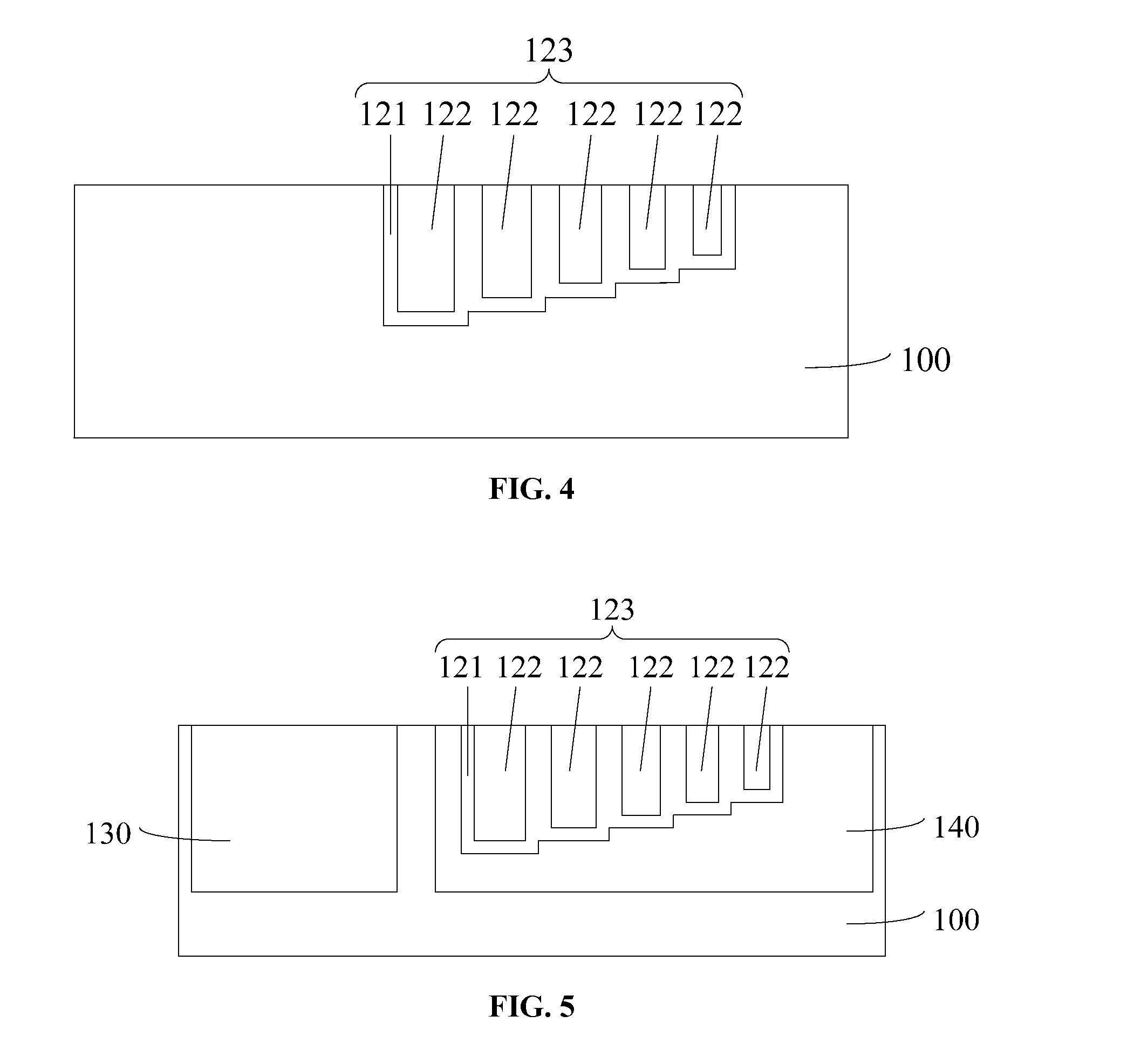
[0011]Reference will now be made in detail to exemplary embodiments of the invention, which are illustrated in the accompanying drawings. Wherever possible, the same reference numbers will be used throughout the drawings to refer to the same or like parts.

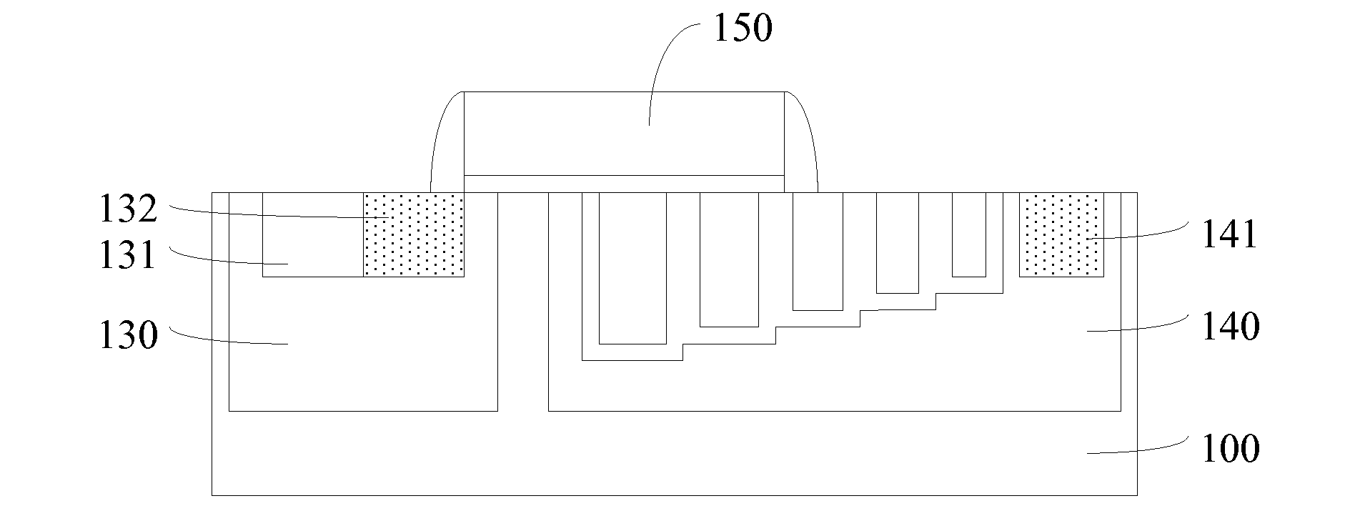
[0012]In a lateral double diffused MOSFET (LDMOSFET) or a lateral insulated gate bipolar transistor (LIGBT); although a higher doping concentration in the drifting region may aid to increase the on-current of the LDMOSFET or the LIGBT, it may reduce the breakdown voltage of the LDMOSFET or the LIGBT. Further, when the doping concentration of the drifting region is relatively small, a surface electric field of a drain junction of the LDMOSFET or the LIGBT may be relatively high, a breakdown may firstly occur at a contact position of a drain region and the drifting region of the LDMOSFET or the LIGBT. When the doping concentration of the drifting region is relatively high, a breakdown may be easy to happen between the drifting region...


PUM


Abstract

A semiconductor device is provided. The semiconductor device includes a semiconductor substrate; and a body region and a drift region formed in the semiconductor substrate. The semiconductor device also includes a bulk region and a source region formed in the body region. Further, the semiconductor device includes a drain region and a first shallow trench isolation structure having a ladder-like bottom formed in the drift region. Further, the semiconductor device also includes a gate structure spanning over an edge of the body region and an edge of the drift region formed on the semiconductor substrate and covering a portion of the first shallow trench isolation structure.

Description

CROSS-REFERENCES TO RELATED APPLICATIONS[0001]This application claims the priority of Chinese patent application No. 201310429750.6, filed on Sep. 18, 2013, the entirety of which is incorporated herein by reference.FIELD OF THE INVENTION[0002]The present invention generally relates to the field of semiconductor manufacturing technology and, more particularly, relates to semiconductor devices and fabrication techniques thereof.BACKGROUND[0003]Currently, lateral double diffused MOSFETs (LDMOSFETs) and lateral insulated gate bipolar transistors (LIGBTs) are widely used in the circuits of logic power managers, electrical chargers, DC-DC converters or AC-DC convertors, etc. With the continuous shrinkage of the critical dimension of CMOS processes, in order to improve the efficiency and reduce the chip size of the LDMOSFETS and the LIGBTs, the on-resistance (Ron) of the LDMOSFETs and the LIGBTs should be as small as possible.[0004]Further, with the continuous shrinkage of the critical dim...

Claims


Application Information

Patent Timeline
Patent Type & Authority Applications(United States)
IPC IPC(8): H01L21/762H01L29/739H01L29/66H01L29/78
CPCH01L21/76229H01L29/7816H01L29/66681H01L29/66325H01L29/7393H01L29/66659H01L29/7835H01L29/0653H01L29/1045
Inventor YANG, GUANGLIYU, QIANRONGWANG, MINGPU, XIANYONG
Owner SEMICON MFG INT (SHANGHAI) CORP
Why Eureka
Try Eureka