Phase change memory and fabrication method

a technology of phase change memory and fabrication method, which is applied in the direction of bulk negative resistance effect devices, basic electric elements, electric devices, etc., can solve the problems of complex and costly fabrication process of conventional pcm

Active Publication Date: 2015-04-02
SEMICON MFG INT (SHANGHAI) CORP +1
View PDF3 Cites 11 Cited by
  • Summary
  • Abstract
  • Description
  • Claims
  • Application Information

AI Technical Summary

Benefits of technology

[0006]One aspect of the present disclosure includes a method for fabricating a phase change memory. A substrate containing a bottom electrode structure through the substrate is provided. The bottom electrode structure has a top surface flushed with a top surface of the substrate. A mask layer is formed on the flushed top surfaces of the substrate and the bottom electrode structure. A first opening is formed in the mask layer to expose the top surface of the bottom electrode structure. A spacer is formed on sidewalls and bottom surface portions of the first opening to expose a surface portion of the bottom electrode structure. The first opening including the spacer therein has a width at a bottom of the first opening less than a width at a top of the first opening. A heating layer is formed at least on the surface portion of the bottom electrode structure exposed by the spacer, the heating layer having a top surface lower than a top surface of the mask layer. A phase change layer is formed on the heating layer to completely fill the first opening. A top electrode is formed on the phase change layer and the mask layer.
[0027]In an exemplary embodiment, during formation of the metal layer 312 above the peripheral metal interconnect structure 102, morphology of the formed second opening 203 can be desirably controlled. This may be because the mask layer 200 that needs to be etched has a thin thickness and simply-structured material layers for forming the second opening 203. Further, since the formed second opening 203 (referring to FIG. 4) has a shallow depth, difficulty of filling the metal material can be reduced when filling the second opening 203 with the metal material. Thus, quality of the formed metal layer can be improved.

Problems solved by technology

However, the fabrication processes for a conventional PCM are complicated and costly.

Method used


Image

  • Phase change memory and fabrication method
  • Phase change memory and fabrication method
  • Phase change memory and fabrication method

Examples


Embodiment Construction

[0012]Reference will now be made in detail to exemplary embodiments of the disclosure, which are illustrated in the accompanying drawings. Wherever possible, the same reference numbers will be used throughout the drawings to refer to the same or like parts.

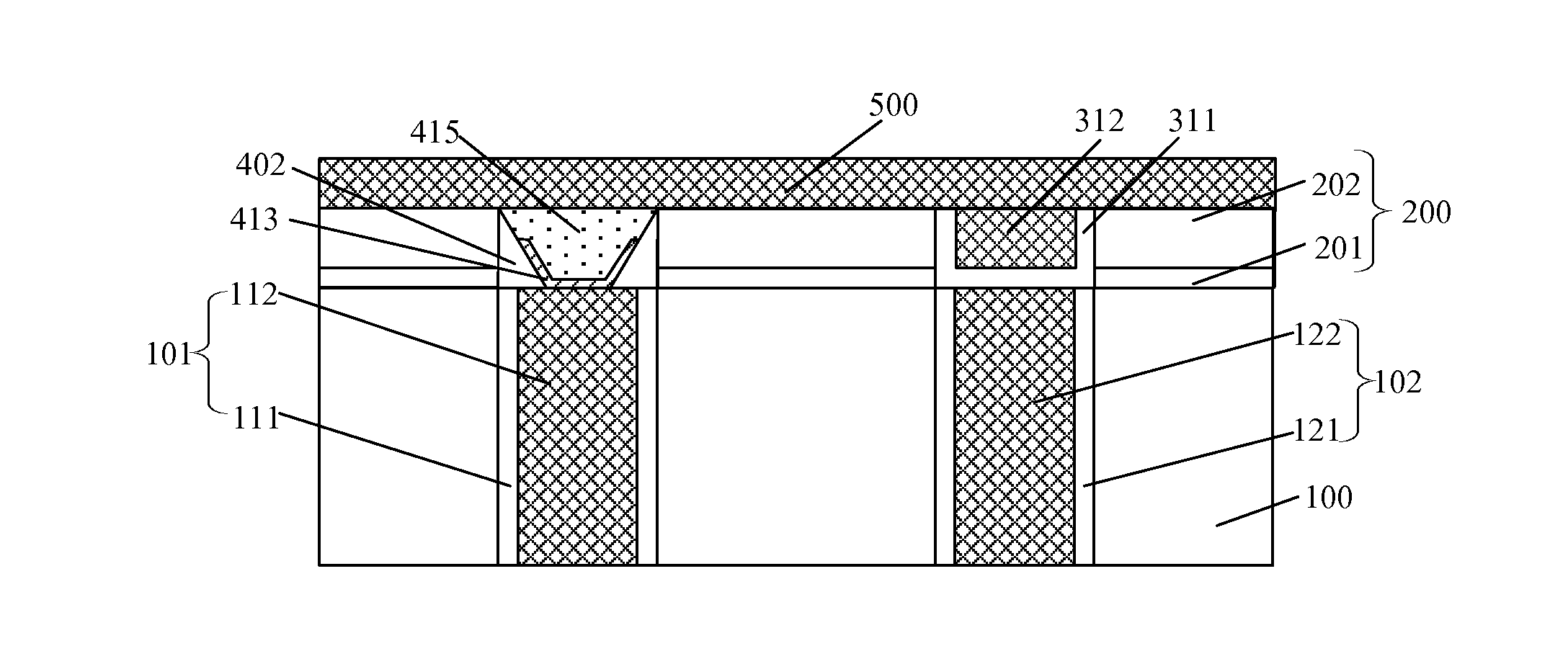
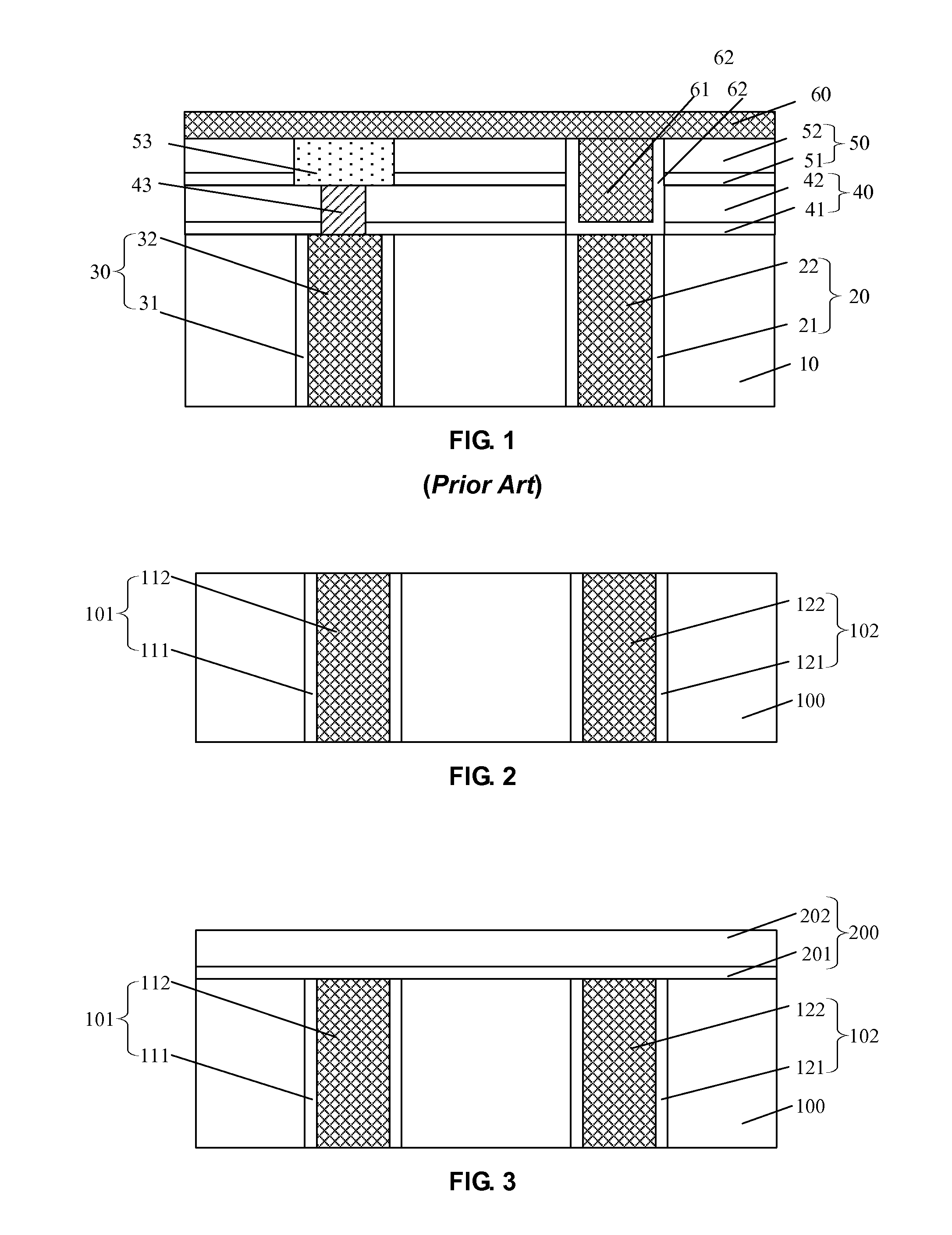
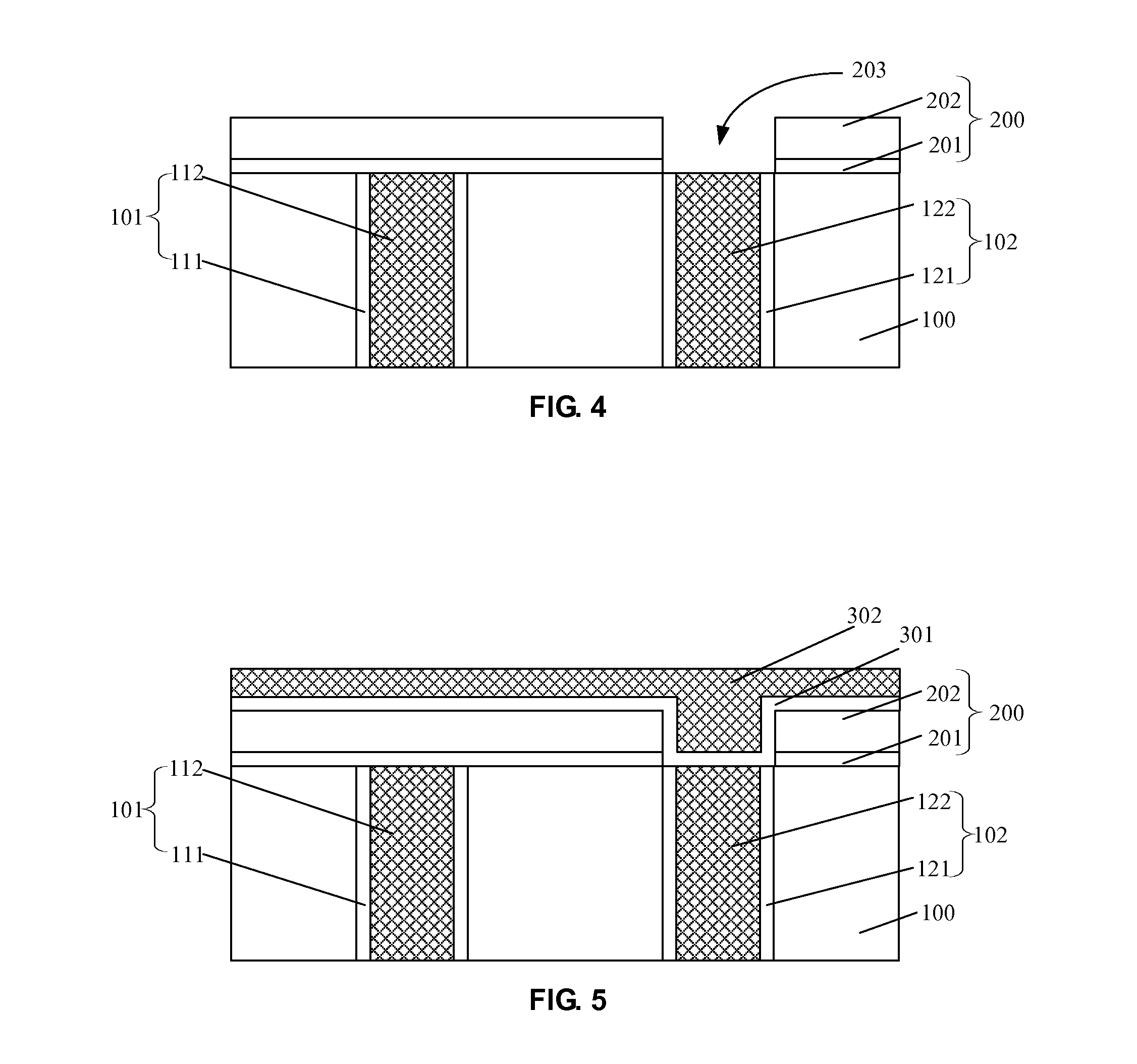
[0013]Conventional processes for forming a PCM (i.e., phase change memory) are complicated and costly. FIG. 1 depicts a conventional PCM. A formation process for such conventional PCM can include providing a substrate 10 and forming a peripheral metal interconnect structure 20 and a bottom electrode 30 in the substrate 10. The peripheral metal interconnect structure 20 includes an interconnect metal layer 22 and an interconnect adhesive layer 21. The bottom electrode 30 includes a bottom electrode metal layer 32 and a bottom electrode adhesive layer 31. A first mask layer 40 covers the substrate 10. The first mask layer 40 includes a first silicon nitride layer 42 and a first silicon oxide layer 42. A first opening in the first ma...


PUM


Abstract

A phase change memory and its fabrication method are provided. A bottom electrode structure is provided through a substrate. A mask layer is formed on the substrate and the bottom electrode structure. A first opening is formed in the mask layer to expose the bottom electrode structure. A spacer is formed on sidewalls and bottom surface portions of the first opening to expose a surface portion of the bottom electrode structure. The first opening including the spacer therein has a bottom width less than a top width. A heating layer is formed at least on the surface portion of the bottom electrode structure exposed by the spacer. A phase change layer is formed on the heating layer to completely fill the first opening. A top electrode is formed on the phase change layer and the mask layer.

Description

CROSS-REFERENCES TO RELATED APPLICATIONS[0001]This application claims the priority to Chinese Patent Application No. CN201310460164.8, filed on Sep. 29, 2013, which is incorporated herein by reference in its entirety.FIELD OF THE DISCLOSURE[0002]The present disclosure generally relates to the field of semiconductor technology and, more particularly, relates to a phase change memory and a method of forming the same.BACKGROUND[0003]Technology of phase change random access memory (PCRAM) is developed from a conception proposed by S. R. Ovshinsky at the end of 1960s that phase change thin film can find applications in phase change storage media. As a recently-emerged non-volatile memory technology, phase change memory (PCM) has advantages over flash memory in many aspects, including read / write speed, read / write times, data retention time, cell area, multiple values, etc. Currently, PCM has become a research focus in the non-volatile memory technology.[0004]A PCM value can be changed by ...

Claims


Application Information

Patent Timeline
Patent Type & Authority Applications(United States)
IPC IPC(8): H01L45/00
CPCH01L45/06H01L45/126H01L45/144H01L45/1683H10N70/8413H10N70/231H10N70/8828H10N70/826H10N70/066
Inventor LI, YING
Owner SEMICON MFG INT (SHANGHAI) CORP
Why Eureka
Try Eureka