

Substrateless packages with scribe disposed on heat spreader
- Summary
- Abstract
- Description
- Claims
- Application Information
AI Technical Summary
Benefits of technology
Problems solved by technology
Method used
Image

Examples
first embodiment
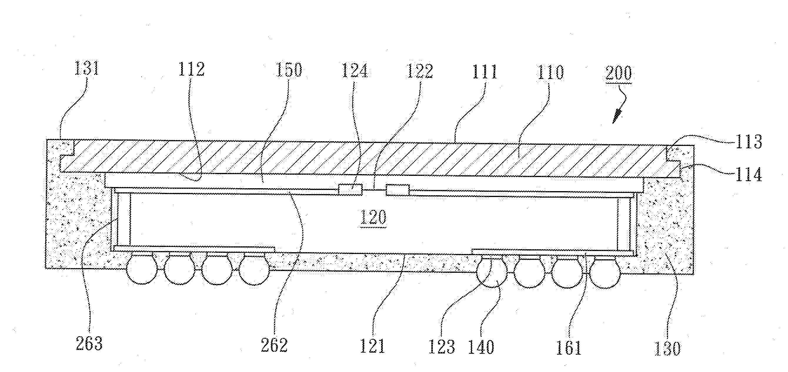
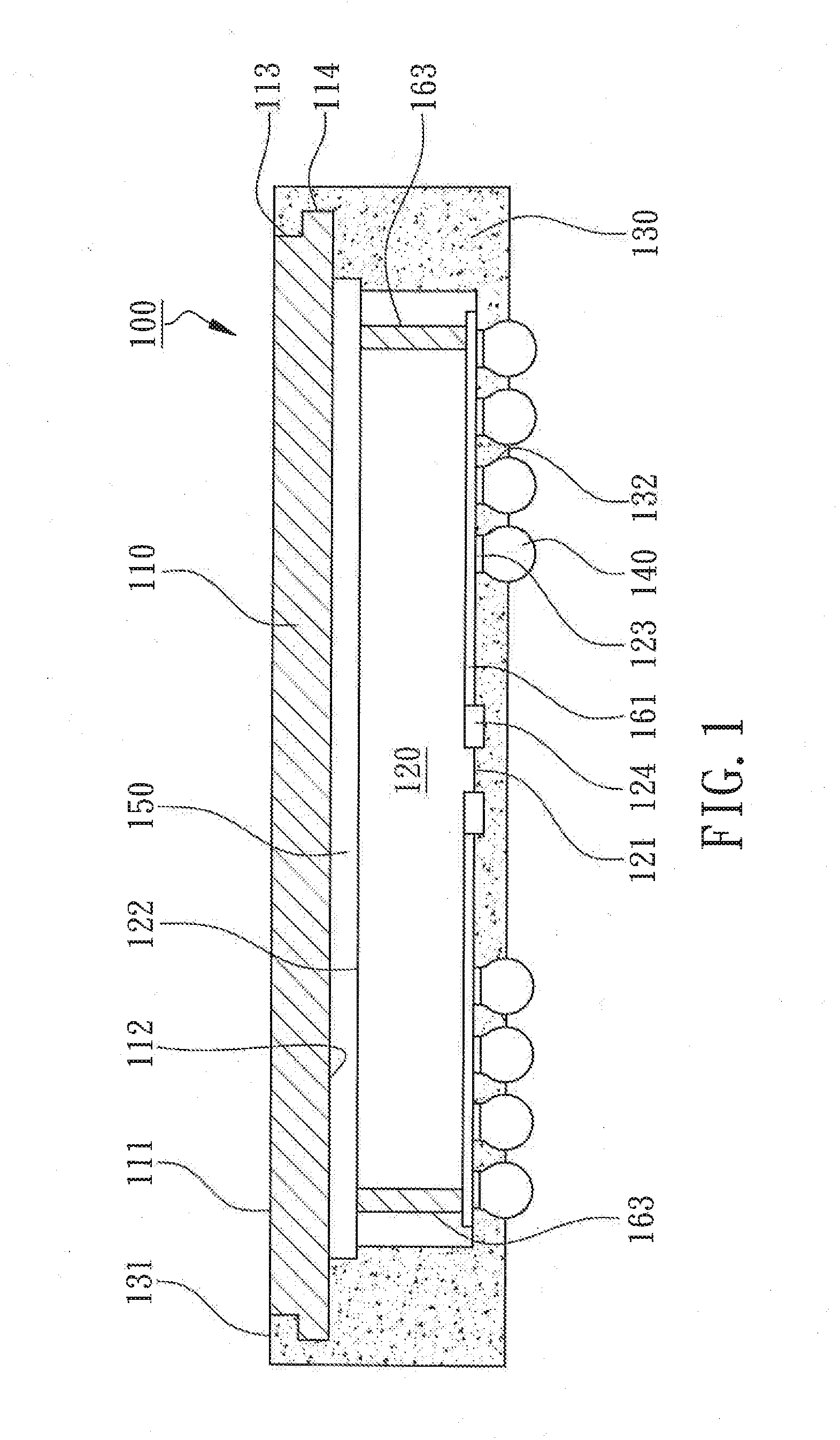
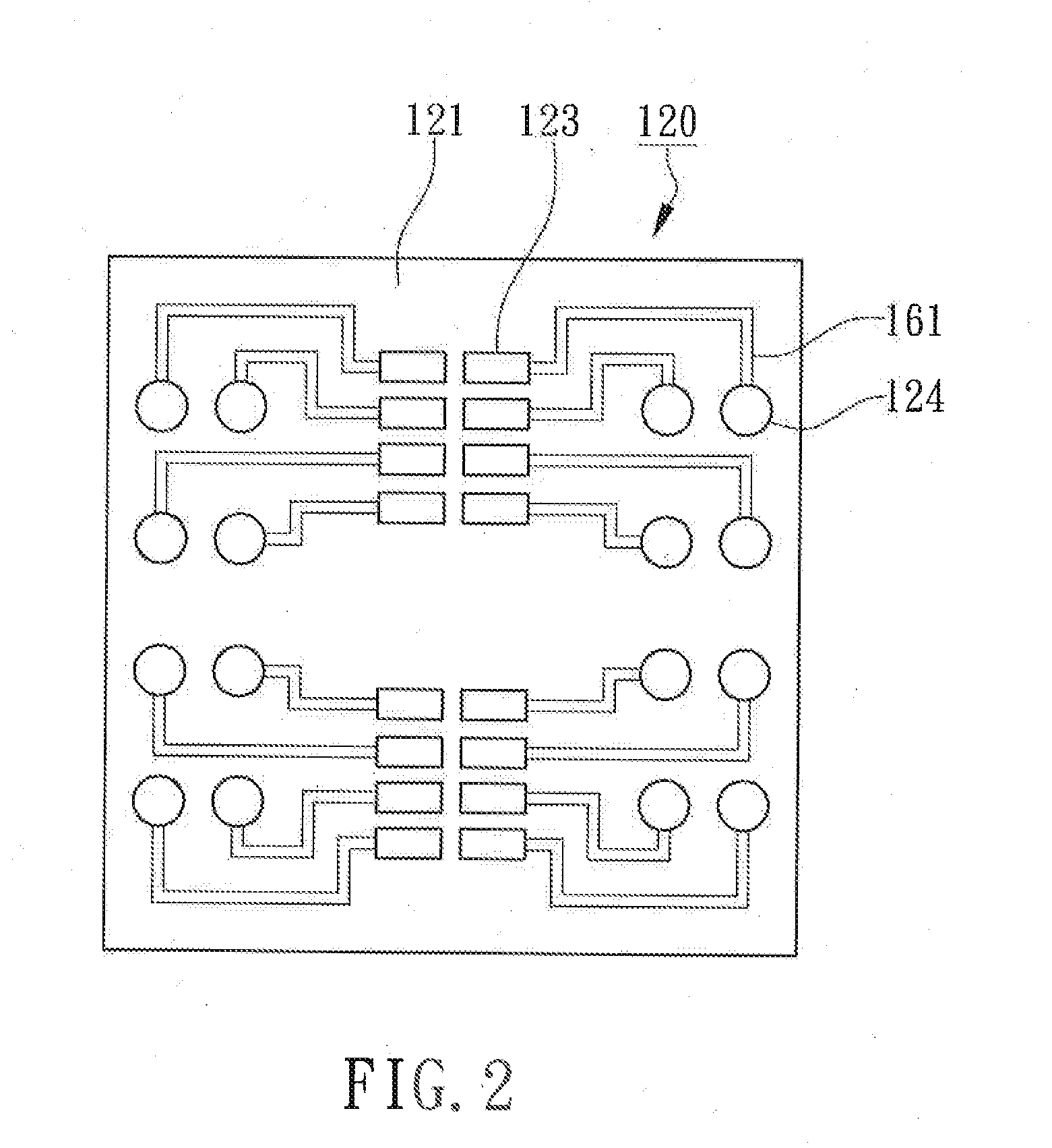
[0015]According to the present invention, a substrateless semiconductor package 100 with a plurality of scribe lines disposed on a heat spreader is illustrated in FIG. 1 for a cross-sectional view. The substrateless semiconductor package 100 primarily comprises a heat spreader 110, a chip 120, and an encapsulant 130. There is no wiring substrate in the package 100 to carry the chip 120. The chip 120 has a first surface 121 and a second surface 122 where, to be more specific, the first surface 121 is the active surface of the chip 120 and the second surface 122 is the backside of the chip 120. The top view of the first surface is illustrated in FIG. 2. The heat spreader 110 has a heat dissipating surface 111 and a die attaching surface 112. FIG. 4A and FIG. 4B are a three-dimensional view of the heat spreader 110 after die-bonding the chip 120 and before package singulation to show the heat dissipating surface 111 and a top view of the die attaching surface 112 of the heat spreader 1...
second embodiment
[0022]According to the present invention, another substrateless semiconductor package 200 with a plurality of scribe lines disposed on a heat spreader is illustrated in FIG. 6 for a cross-sectional view. The substrateless semiconductor package 200 primarily comprises a heat spreader 110, a chip 120, and an encapsulant 130. The chip 120 has a first surface 121 and a second surface 122 where, to be more specific, the first surface 121 is the backside of the chip 120 and the second surface 122 is the active surface of the chip 120. The heat spreader 110 has a heat dissipating surface 111 and a die attaching surface 112. A plurality of scribe line grooves 113 are formed on the heat dissipating surface 111 of the heat spreader 110 where a plurality of first openings 114 are formed inside the scribe line grooves 113 to penetrate through the heat spreader 110 so that the scribe line grooves 113 are physically connected to the die attaching surface 112. The second surface 122 of the chip 12...
PUM
 Abstract
Description
Claims
Application Information