Gate signal line drive circuit and display device

a technology of signal line drive and display device, which is applied in the direction of digital storage, instruments, computing, etc., can solve the problems of power consumption increase, brightness reduction, and degraded display screen quality

Active Publication Date: 2015-04-02
JAPAN DISPLAY INC
View PDF2 Cites 4 Cited by
  • Summary
  • Abstract
  • Description
  • Claims
  • Application Information

AI Technical Summary

Benefits of technology

[0014]The present invention has been made in view of the above problem, and therefore aims at providing a gate signal line drive circuit that reduces a power consumption, and a display device using the gate signal line drive circuit.
[0021]According to the present invention, there are provided the gate signal line drive circuit whose power consumption is reduced, and the display device using the drive circuit.

Problems solved by technology

However, since a charge and discharge current flows in the transistor T5 due to a parasitic capacitance provided in the transistor T5 every time a voltage of the basic clock signal Vn changes, a power consumption increases.
However, as indicated by a dashed line in FIG. 17, if the falling waveform of the gate signal Gn is increasingly blunted, the gate signal Gn does not sufficiently drop to the low voltage even after the pixel circuit writes the pixel, the pixel voltage held by the pixel circuit is varied by rewrite without sufficiently turning off the switching transistor of the pixel circuit, and the quality of a display screen is degraded, for example, the brightness is reduced.

Method used


Image

  • Gate signal line drive circuit and display device
  • Gate signal line drive circuit and display device
  • Gate signal line drive circuit and display device

Examples


first embodiment

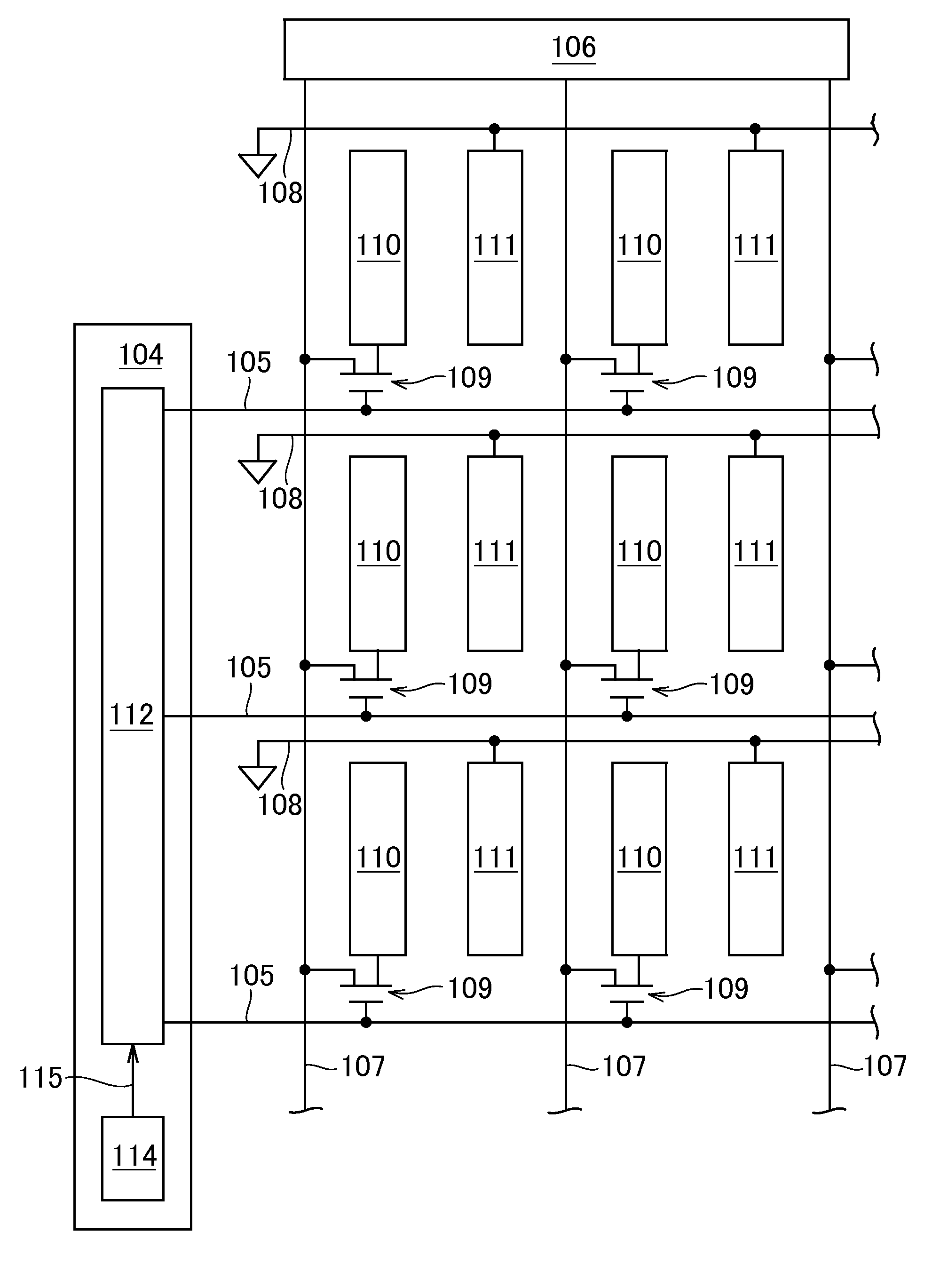
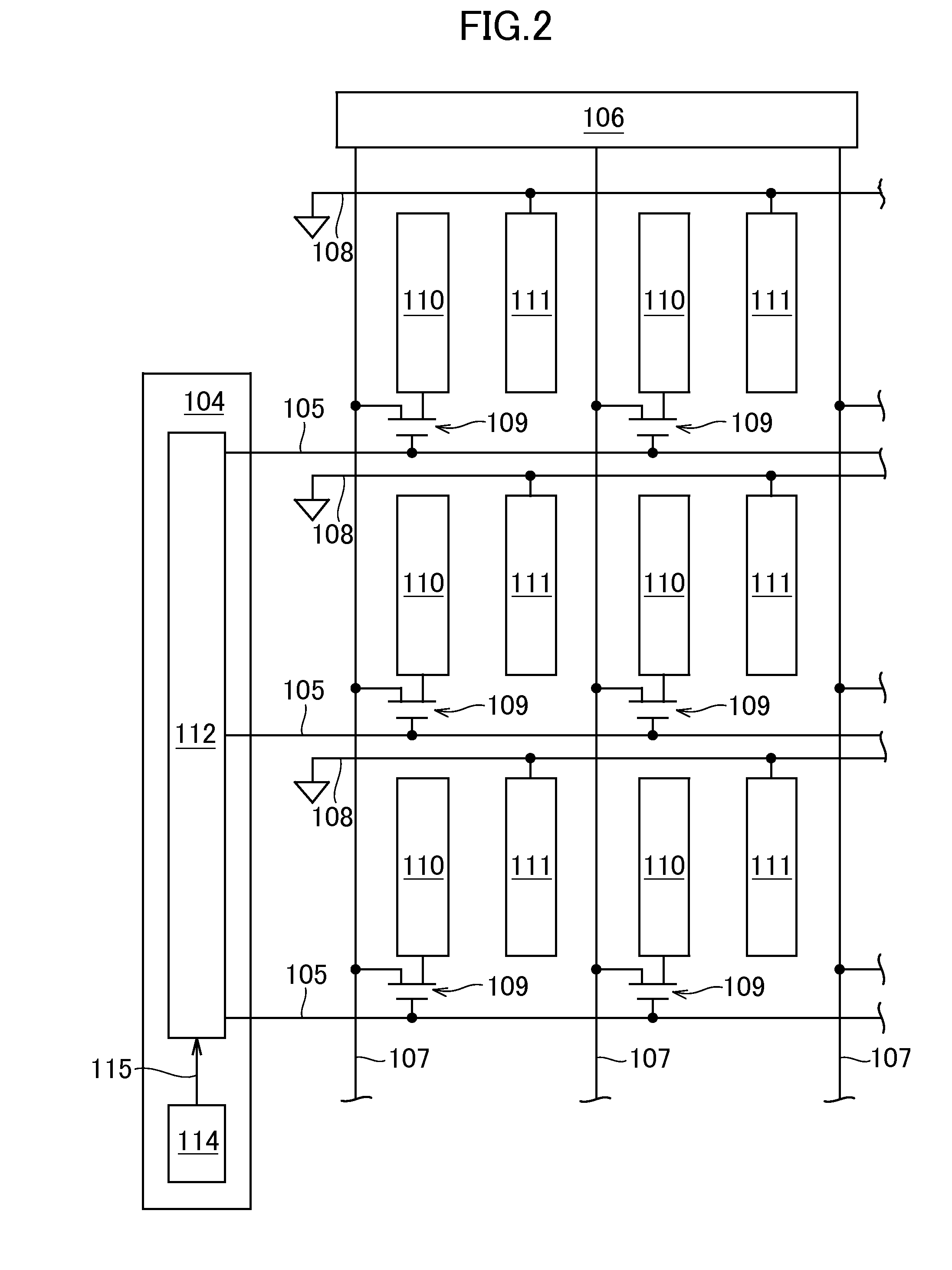
[0040]A display device according to a first embodiment of the present invention is, for example, an IPS (in-plane switching) liquid crystal display device. FIG. 1 is a perspective view of an overall liquid crystal display device according to the first embodiment. As illustrated in FIG. 1, the liquid crystal display device according to the embodiment includes a TFT substrate 102 on which gate signal lines 105, video signal lines 107, pixel electrodes 110, a common electrode 111, and TFTs 109, which will be describe later, are arranged, a filter substrate 101 that faces the TFT substrate 102, and has color filters disposed thereon, a liquid crystal material that is sealed in an area sandwiched between those substrates, and a backlight 103 that is located in contact with a side of the TFT substrate 102 opposite to the filter substrate 101 side.

[0041]FIG. 2 is a conceptual diagram illustrating an equivalent circuit of the TFT substrate 102 according to this embodiment. Referring to FIG....

second embodiment

[0079]An n-th basic circuit 113-n according to a second embodiment of the present invention is different from that of the first embodiment in that a signal input to the gate of the transistor T5B, which is the first low voltage application on control element, is input from a node N1n+1 of an (n+1)-th basic circuit 113-(n+1). Also, a gate signal line low voltage supply circuit 14, provided in the n-th basic circuit 113-n is arranged on a side of the display area 120 opposite to the main circuit of the n-th basic circuit 113-n. The other structures of the gate signal line drive circuit 104 according to this embodiment are identical with those of the first embodiment.

[0080]FIG. 7 is a schematic diagram illustrating a configuration of a gate signal line drive circuit 104 according to this embodiment. The gate signal line drive circuit 104 according to this embodiment includes an even shift register circuit 112A that outputs gate signals to respective even-numbered gate signal lines 105 ...

third embodiment

[0086]A gate signal line drive circuit 104 according to a third embodiment of the present invention is different in the configuration of the basic circuits 113 from that of the first or second embodiment, and also different in the basic clock signal to be input from that of the first or second embodiment. On the other hand, the other structures are identical with those of the first or second embodiment.

[0087]FIG. 10 is a circuit diagram of an n-th basic circuit 113-n according to this embodiment. The n-th basic circuit 113-n according to this embodiment includes a main circuit portion 15, and a gate signal line low voltage supply circuit 14.

[0088]First, the main circuit portion 15 of the n-th basic circuit 113-n will be described. The n-th basic circuit 113-n according to this embodiment is different from the n-th basic circuit 113-n according to the first embodiment illustrated in FIG. 4 in that the input terminal IN2, the transistors T3, T7, and the retentive capacitor C3 are not ...


PUM


Abstract

A gate signal line drive circuit whose power consumption is reduced, is provided. In the gate signal line drive circuit having plural basic circuits outputting respective gate signals, each basic circuit includes a high voltage application switching element to which a first basic clock signal having high voltage in a signal high period is input, a low voltage application switching element that turns on at timing starting a signal low period, and outputs a low voltage, and a first low voltage application on control element having an input terminal to which a second basic clock signal subsequent to the first basic clock signal is input, and which turns on according to the signal high period, and outputs the voltage of the second basic clock signal to the control terminal of the low voltage application switching element.

Description

CROSS-REFERENCE TO RELATED APPLICATION[0001]The present application claims priority from Japanese application JP 2013-202602, filed on Sep. 27, 2013, the content of which is hereby incorporated by reference into this application.BACKGROUND OF THE INVENTION[0002]1. Field of the Invention[0003]The present invention relates to a gate signal line drive circuit and a display device using the drive circuit. In particularly, the present invention relates to a reduction in power consumption in a gate signal line drive circuit.[0004]2. Description of the Related Art[0005]Up to now, for example, liquid crystal display devices may employ a system in which a shift register circuit disposed in a gate signal line drive circuit that scans gate signal lines is formed on the same substrate as that of thin film transistors (hereinafter referred to as “TFT”) which are arranged in a pixel area of a display screen, that is, a shift register built-in system.[0006]The shift register circuit disposed in th...

Claims


Application Information

Patent Timeline
Patent Type & Authority Applications(United States)
IPC IPC(8): G09G3/36
CPCG09G3/3677G09G3/3648G09G2330/021G09G2310/0289G09G2310/0286G09G2310/0202G09G2300/0426G09G2310/08G11C19/28
Inventor OCHIAI, TAKAHIROMIYAMOTO, MOTOHARUHOSHIBA, MASAHIRO
Owner JAPAN DISPLAY INC
Why Eureka
Try Eureka