Method for fabricating nano-patterned substrate for high-efficiency nitride-based light-emitting diode

a technology nano-patterned substrates, which is applied in the direction of semiconductor/solid-state device manufacturing, electrical apparatus, semiconductor devices, etc., can solve the problems of low light extraction efficiency in comparison with internal photon efficiency, generation of heat in/of devices, and insufficient improvement of nitride-based light-emitting diodes to meet such needs. , to achieve the effect of improving product performance, increasing production yield and economic feasibility

Active Publication Date: 2015-04-02
HUNET PLUS
View PDF0 Cites 8 Cited by
  • Summary
  • Abstract
  • Description
  • Claims
  • Application Information

AI Technical Summary

Benefits of technology

[0021]In the present invention, as a diameter and a cycle of a pattern of a substrate for a light emitting diode are reduced to a nano grade, internal photon efficiency and light manufacturing a nano to micron sized pattern on a substrate using a nano print (or imprint) lithography technique, which is an economic and non-optical patterning technique, is presented. Since the nano print (or imprint) technique enables transfer of a pattern onto a large area through an economic and simple process without necessity of expensive exposure equipment, production yield may be increased. In particular, since the patterning for the light emitting diode does not require precise alignment, the nano print (or imprint) process, which is a direct pattern transfer method, may be appropriately applied, and a sub-micron pattern may be easily formed. Accordingly, in comparison with the conventional photolithography process for manufacturing the PSS, when the nano print (o

Problems solved by technology

However, performance of the nitride-based light emitting diode is not being sufficiently improved to satisfy such needs.
In recent times, while the internal photon efficiency of the nitride-based light emitting diode has been largely improved due to development of the epitaxial growth technique, the light extraction efficiency is very low in comparison with the internal photon efficiency.
In

Method used


Image

  • Method for fabricating nano-patterned substrate for high-efficiency nitride-based light-emitting diode
  • Method for fabricating nano-patterned substrate for high-efficiency nitride-based light-emitting diode
  • Method for fabricating nano-patterned substrate for high-efficiency nitride-based light-emitting diode

Examples


Embodiment Construction

[Technical Problem]

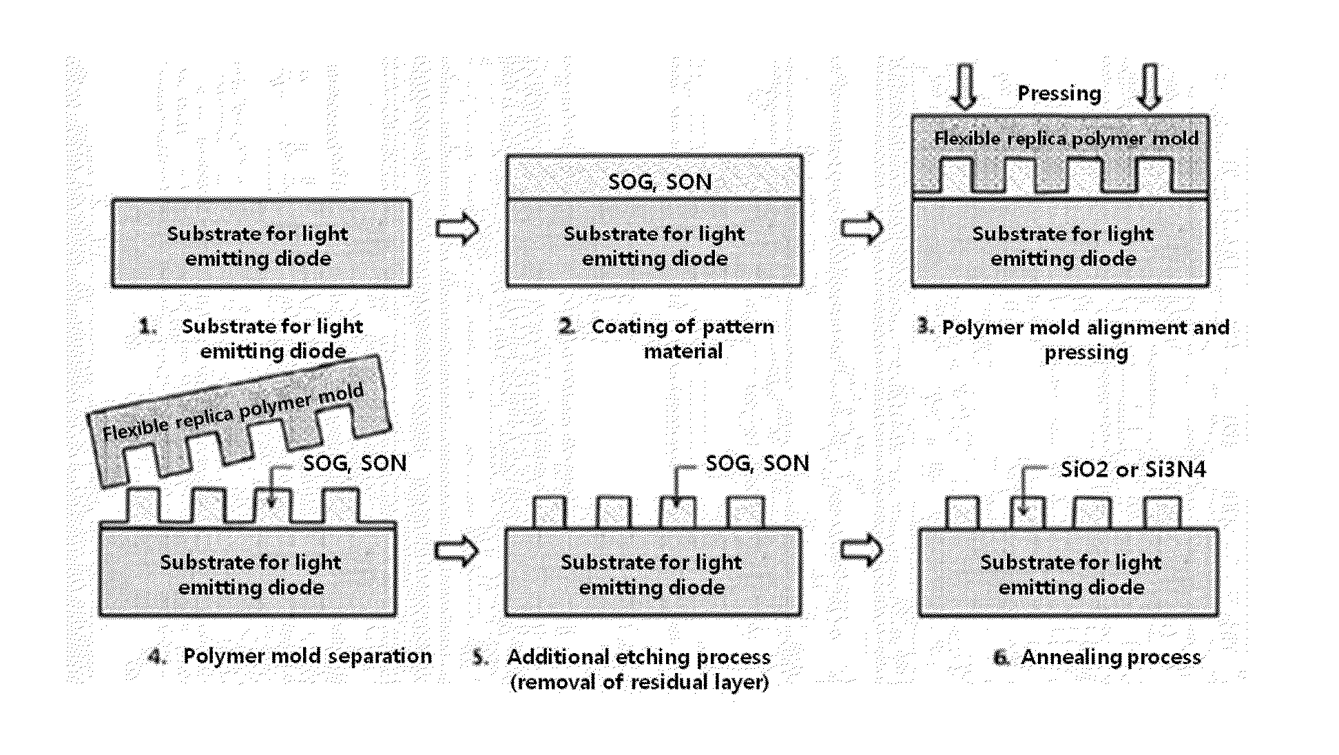
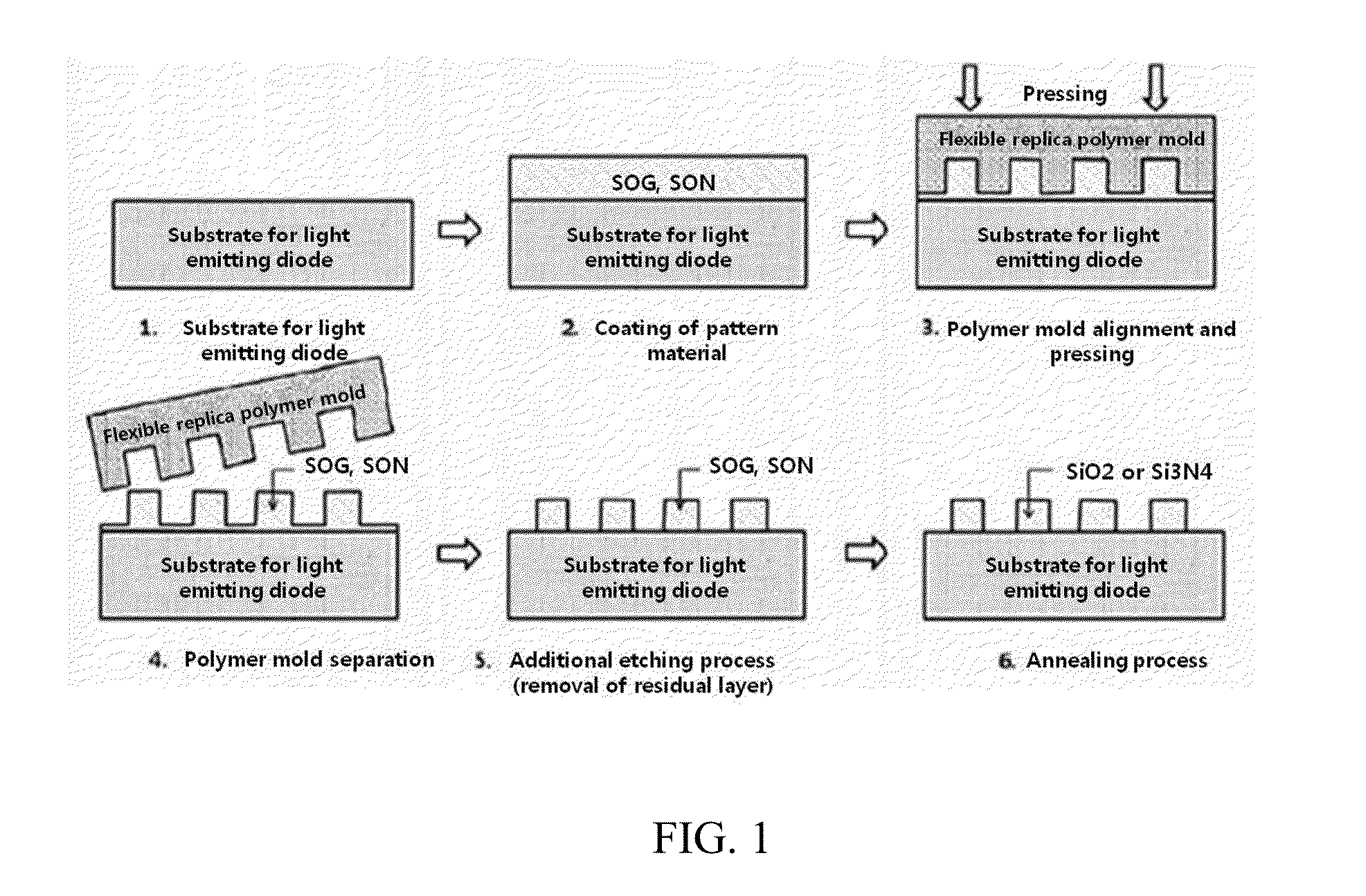
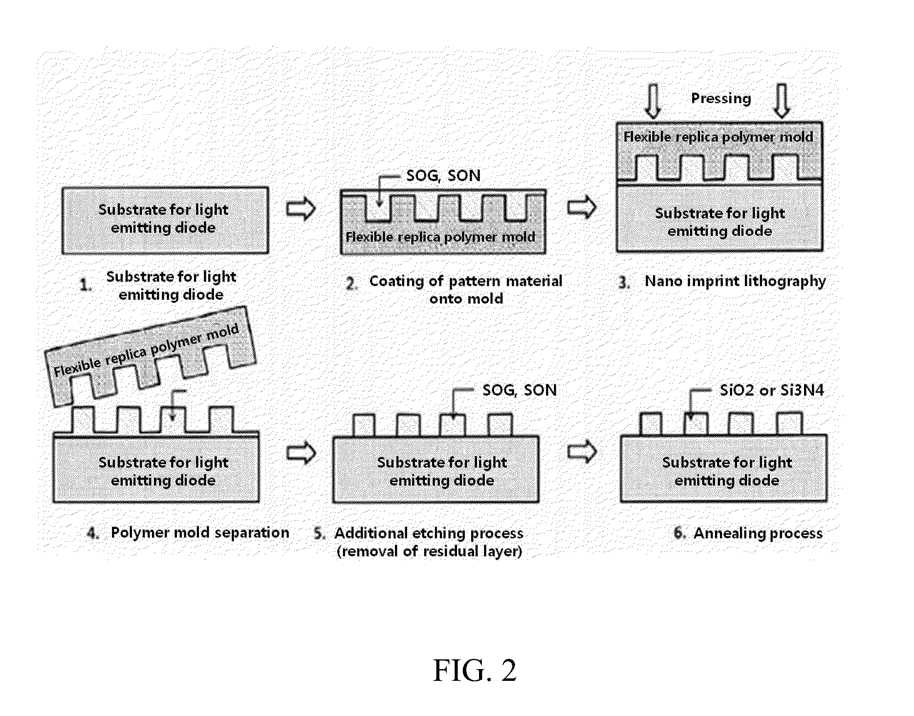
[0006]Currently, the patterned sapphire substrate (PSS) is mainly manufactured through a photolithography process and a dry and wet etching process, and specification of most of the patterns is about several microns. An extent in improvement of the light extraction efficiency of the light emitting diode due to the diffused reflection of the light is largely varied according to size, shape, cycle, or the like, of the patterns. It is known that, when a nano photonic crystal pattern is applied to a light emitting region of the light emitting diode, light extraction is largely increased. Accordingly, a diameter and cycle of the micro pattern of a conventionally commercialized PSS should be reduced to a nano grade to improve the efficiency of the light emitting device, and a shape of the pattern should (also) be optimized.

[0007]Since the photolithography, which is a patterning technique used for manufacturing of the PSS, is expensive and application of the nano to micr...


PUM


Abstract

Provided is a method of manufacturing a substrate for a light emitting diode including a convex section forming step and a crystallization/crystallizing step. According to the method and the substrate for the light emitting diode, light extraction is significantly improved and nano to micron sized pattern, economically formed.

Description

TECHNICAL FIELD[0001]The present invention is provided to: economically manufacture a nano to micron sized pattern on a substrate of a light emitting diode including a convex section, which includes any one selected from the group consisting SiO2, Si3N4, and a combination thereof, using a nano printing or nano imprinting process; efficiently form the nano to micron sized pattern on the substrate of the light emitting diode formed of sapphire monocrystal and the like, using this process; and form gallium nitride or the like having a small crystal defect—thereby significantly increasing performance of the light emitting diode.BACKGROUND ART[0002]A light emitting diode is receiving attention as a light source for future lighting and widely used as a light source in various fields at present due to a long lifespan, small power consumption, and environment-friendliness in comparison with lighting fixtures such as conventional fluorescent lamp, incandescent lamp, and so on. In particular,...

Claims


Application Information

Patent Timeline
IPC IPC(8): H01L33/00H01L33/22
CPCH01L33/007H01L2933/0033H01L33/22H01L33/20H01L21/0237H01L21/0254H01L21/02639H01L21/02647H01L21/3105H01L21/311H01L33/12H01L21/02356
Inventor CHA, HYUK-JINLEE, HEONCHOI, EUN-SEO
Owner HUNET PLUS
Why Eureka
Try Eureka