High Electron Mobility Transistors with Minimized Performance Effects of Microcracks in the Channel Layers

a technology of high electron mobility and transistors, applied in the direction of semiconductor devices, basic electric elements, electrical appliances, etc., can solve the problems of mismatch between thermal expansion coefficients and lattices, limited performance of silicon power devices, and affecting the electronic properties of films

Active Publication Date: 2015-04-16
SHIH ISHIANG +3
View PDF0 Cites 11 Cited by
  • Summary
  • Abstract
  • Description
  • Claims
  • Application Information

AI Technical Summary

Problems solved by technology

However, the performance of these silicon power devices is still limited mainly due to their limited breakdown electric field.
However, due to the difference between the III-nitrides materials and the sapphire or SiC substrates used for these devices, there is often a mismatch in their thermal expansion coefficients and their lattices.
These strain or stresses may lead to microcracks in the epitaxial III-nitride layers and the electronic properties of the films may be affected due to the presence of the microcracks.
It should be noted that these microcracks are often too small to be unequivocally observed under simple optical microscopes with a low magnification.
Although current III-nitride devices are mainly manufactured on sapphire or SiC substrates, both sapphire and SiC substrates are more difficult or expensive to manufacture due to the nature of the compounds and their high melting points.
While vigorous recent efforts have been made on research and development of III-nitride epitaxial growth on silicon wafer and device fabrication, there are still obstacles to be overcome.
The microcracks can degrade the electronic performance and reliability of the fabricated devices and circuits.

Method used


Image

  • High Electron Mobility Transistors with Minimized Performance Effects of Microcracks in the Channel Layers
  • High Electron Mobility Transistors with Minimized Performance Effects of Microcracks in the Channel Layers
  • High Electron Mobility Transistors with Minimized Performance Effects of Microcracks in the Channel Layers

Examples


Embodiment Construction

Occurrence of Microcracks:

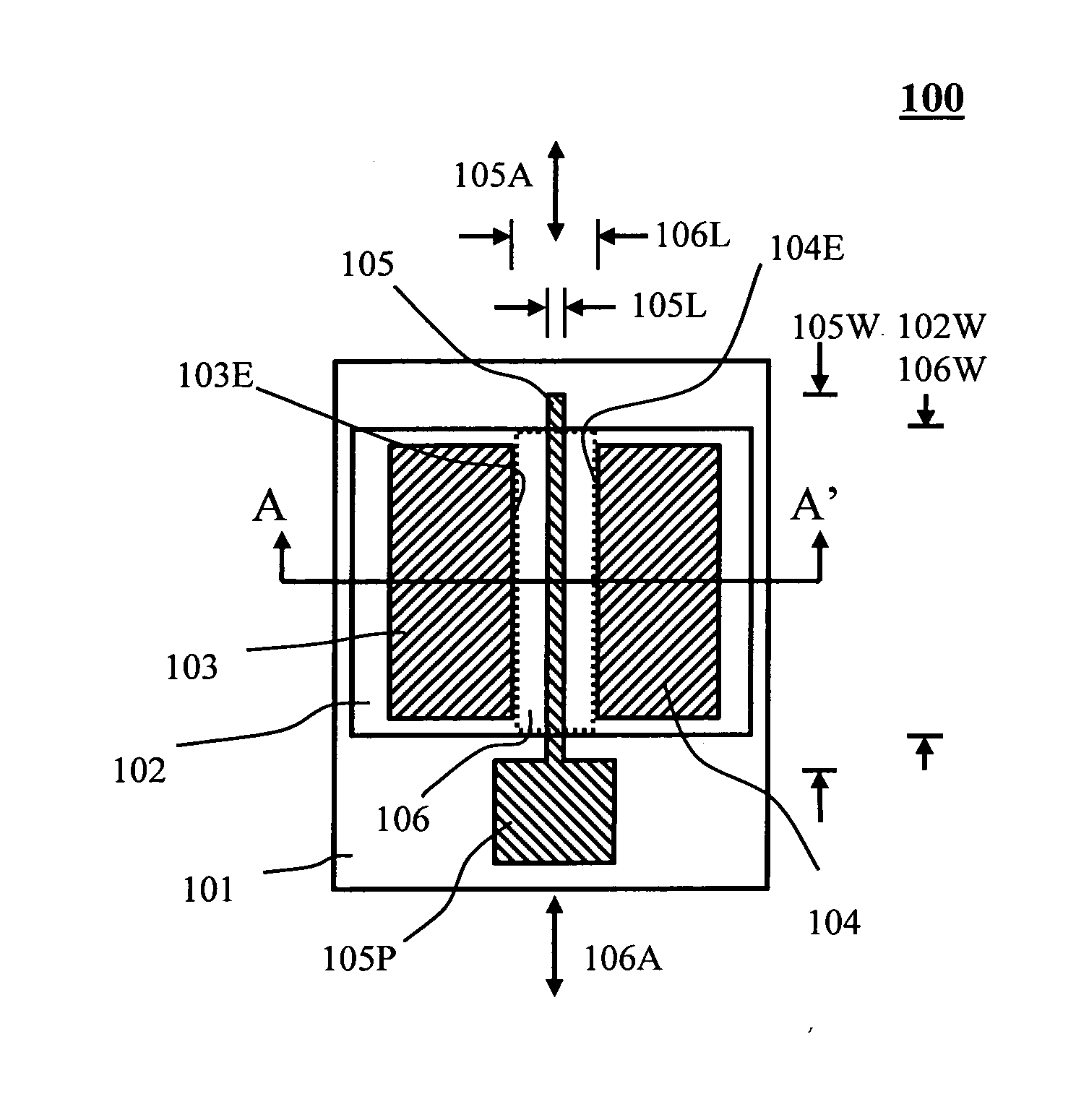
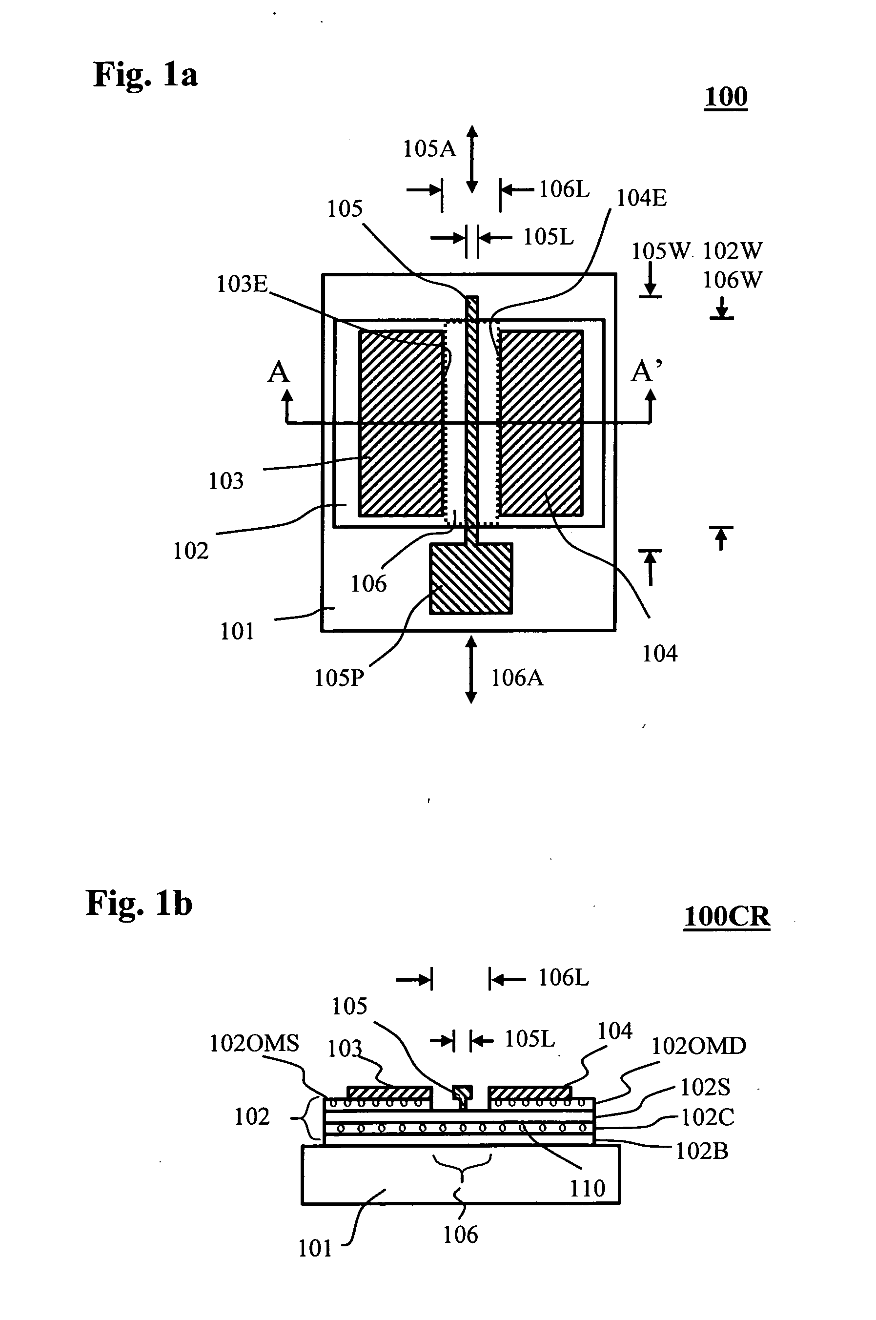
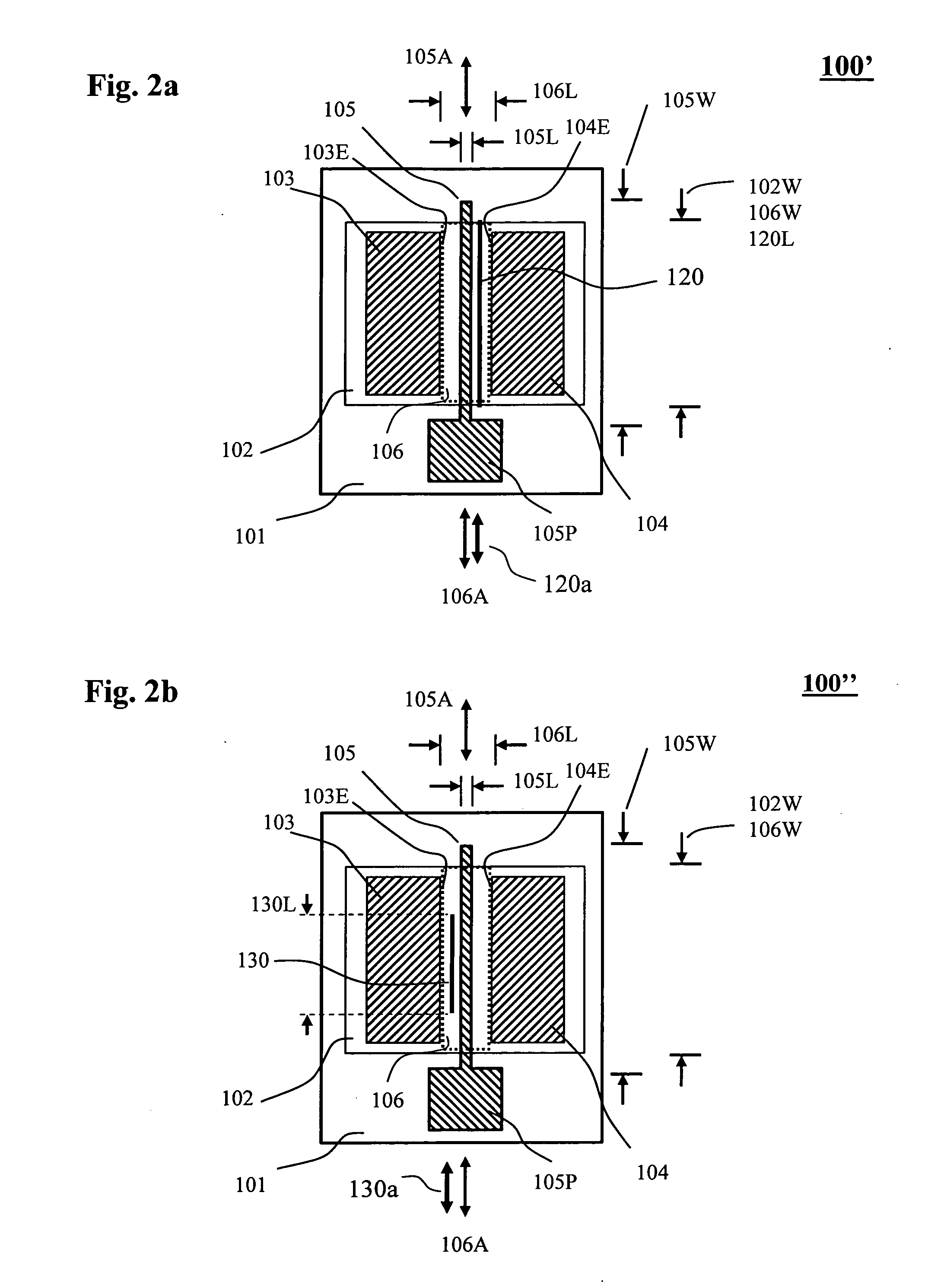
[0022]The devices considered in this invention are based on III-nitrides films deposited on substrates such as silicon, sapphire and silicon carbide. Take Si wafers as an example, the deposition of the III-nitride films may be made on (111) plane or (100) plane. During the cooling period after the deposition, tensile stresses are induced in the deposited III-nitride epitaxial layers. For example, in AlGaN—GaN—Si with undoped AlGaN and undoped GaN layers, the tensile stress induced in the AlGaN layer leads to charge polarization in the AlGaN layer. Due to the charge polarization, positive polarization charges are induced in the AlGaN near the GaN layer whereas negative polarization charges are induced on or near the top surface of the AlGaN layer. The positive polarization charges induce negative mobile charges (free carriers) of equal amount on the top of the GaN layer, forming a mobile charge sheet for a conduction channel of the transistor to be formed. T...


PUM

PropertyMeasurementUnit
lengthaaaaaaaaaa
lengthaaaaaaaaaa
angle θAaaaaaaaaaa

Abstract

In HEMTs based on III-nitrides epitaxial films or GaAs, AlGaAs and InGaAs epitaxial films, unwanted microcracks are often formed in the composite epitaxial layers in the channel region during fabrication and operation. These microcracks are caused by strain or stresses due to lattice mismatch and thermal expansion coefficient differences between materials and substrate's. Those microcracks will bring about an increase in source to drain resistance and lead to performance and reliability degradation of the HEMTs and the MMICs containing them. The present invention provides HEMTs with minimized effects of the unwanted microcracks by aligning the channel region long axis to a certain direction so that the channel region long axis forms a right angle with axis of at least one type of the microcracks.

Description

FIELD OF INVENTION[0001]The present invention is related to transistor devices and MMICs for power switching and microwave amplification and switching. Specifically, it is related to transistor devices having minimized performance effects of microcracks formed in the channel layers during fabrication and operation.BACKGROUND OF THE INVENTION[0002]For power switching, devices based on a metal-oxide-semiconductor (MOS) structure, an insulated gate bipolar transistor (IGBT) structure and a lightly doped drain metal-oxide-semiconductor (LDMOS) structure are commonly used. Power devices based on the MOS structure are mainly used in domestic units which are operated at a few hundreds volts. Power devices based on IGBT are for high power switching in applications including AC to DC or DC to AC conversion and are designed to sustain high voltages up to several kilovolts. Power devices based on LDMOS are for intermediate power level applications. Current MOS, LDMOS and IGBT devices are manuf...

Claims


Application Information

Patent Timeline
Patent Type & Authority Applications(United States)
IPC IPC(8): H01L29/778
CPCH01L29/7787H01L29/045H01L29/2003
Inventor SHIH, ISHIANGQIU, CHUNONGQIU, CINDY X.SHIH, YI-CHI
Owner SHIH ISHIANG
Why Eureka
Try Eureka