Integrated circuit and operating method for the same

Active Publication Date: 2015-04-23
MACRONIX INT CO LTD
View PDF32 Cites 1 Cited by
  • Summary
  • Abstract
  • Description
  • Claims
  • Application Information

AI Technical Summary

Benefits of technology

This patent describes an integrated circuit that includes a stacked structure and a conductive structure. The conductive structure is disposed above the stacked structure and electrically connected to the conductive strip. The conductive structure and the conductive strip have various gap distances between corresponding points of different pairs according to a basic axis. The patent also describes an operating method for the integrated circuit that involves applying a first voltage to the conductive structure of the dummy region and a second voltage to the second conductive layer of the dummy region, where the first voltage is equal to the second voltage. The technical effect of this patent is to provide a more efficient and precise method of operating the integrated circuit.

Problems solved by technology

These variations can lead to endurance problems with the memory cells and to other complexities.
These variations in capacitance affect the global bit line voltages during read, program and erase operations, and can result in specification requirements, such as larger read margins between programmed and erased states, and slower sensing times to account for worst case capacitances.

Method used


Image

  • Integrated circuit and operating method for the same
  • Integrated circuit and operating method for the same
  • Integrated circuit and operating method for the same

Examples


Embodiment Construction

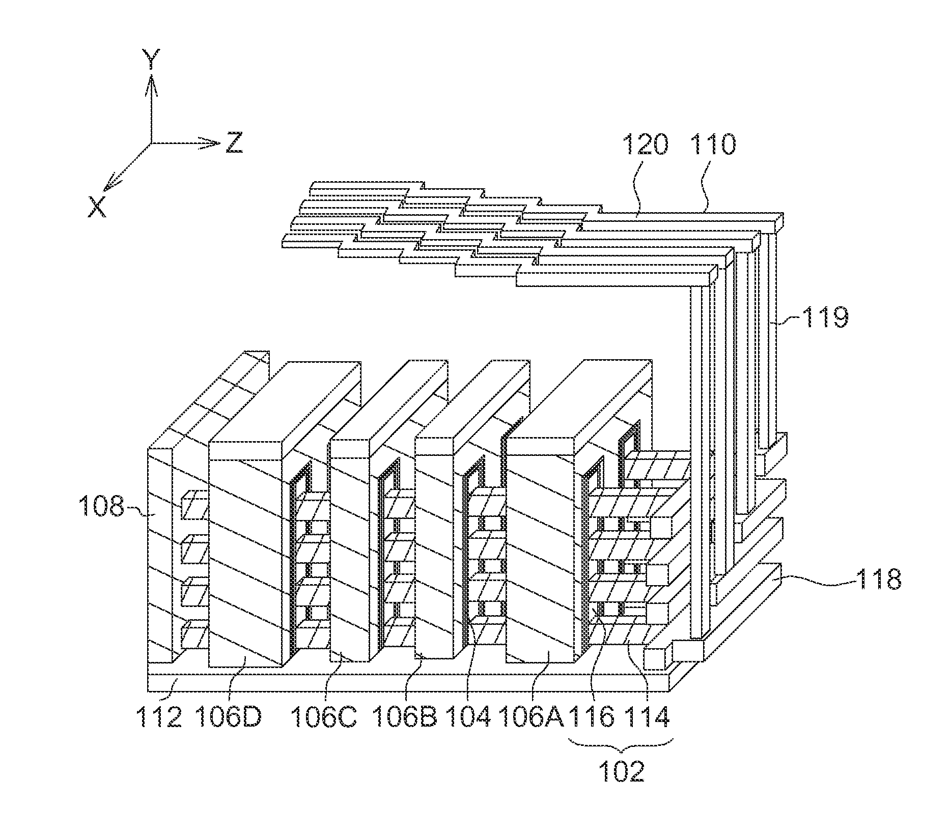
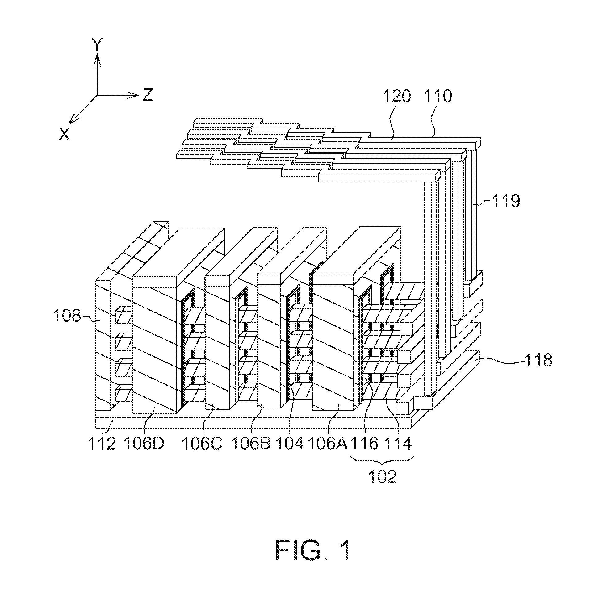
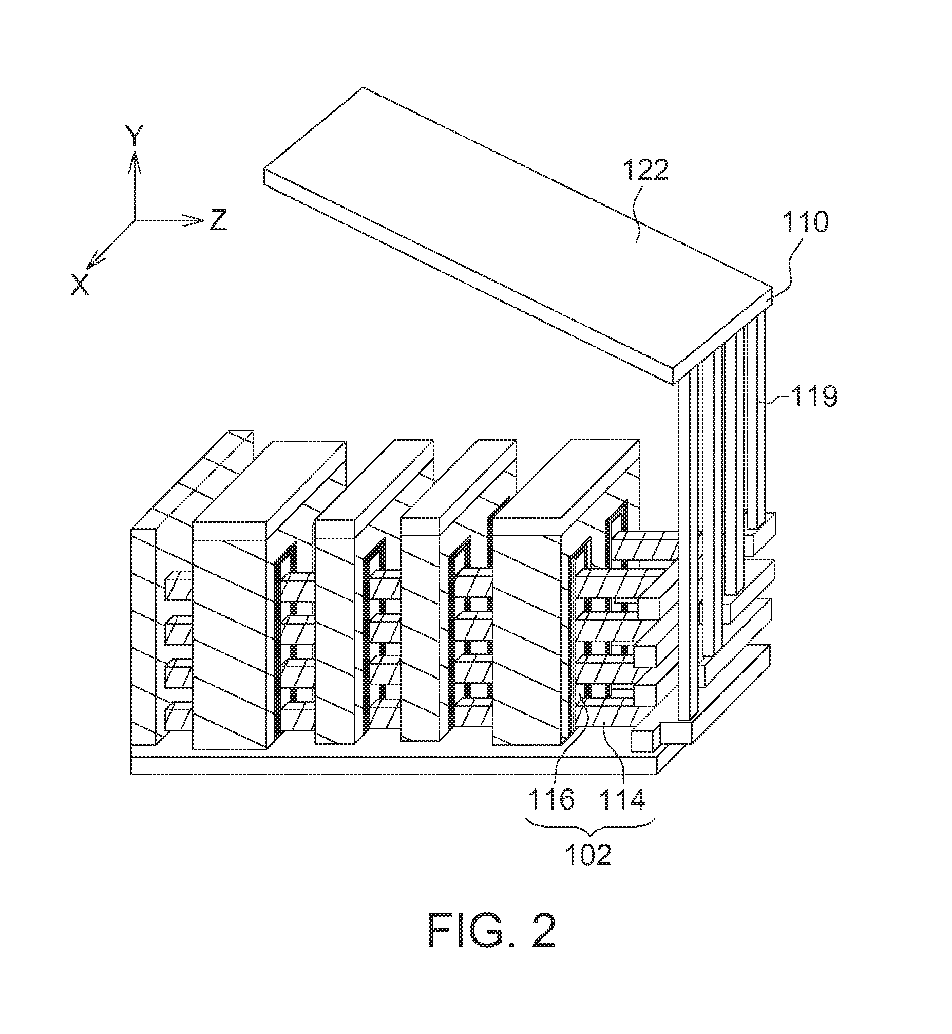
[0016]FIG. 1 shows an integrated circuit according to one embodiment. The integrated circuit comprises a 3D memory stack comprising stacked structures 102, a dielectric layer 104, first conductive layers 106A, 106B, 1060. 106D and a second conductive layer 108. The integrated circuit also comprises a conductive structure 110.

[0017]Referring to FIG. 1, the stacked structure 102 of different rows, for example extending along a Z direction, are separated from each other and disposed on a substrate 112. Each of the stacked structures 102 comprises conductive strips 114 and dielectric strips 116 stacked in a stagger manner and having a straight strip shape. The dielectric strip 116, similar with the conductive strip 114, is a straight strip structure extended continuously. FIG. 1 does not show portions of the dielectric strip 116 between the first conductive layers 106A, 106B, 1060 and 1060 and the second conductive layer 108 for the sake of brevity of the integrated circuit of one embod...


PUM


Abstract

An integrated circuit and an operating method for the same are provided. The integrated circuit comprises a stacked structure and a conductive structure. The stacked structure comprises a conductive strip. The conductive structure is disposed above the stacked structure and electrically connected to the conductive strip. The conductive structure and the conductive strip have various gap distances between corresponding points of different pairs according to a basic axis.

Description

BACKGROUND[0001]1. Technical Field[0002]The disclosure relates to an integrated circuit and an operating method for the same, and more particularly to an integrated circuit having a conductive structure and an operating method for the same.[0003]2. Description of the Related Art[0004]As critical dimensions of devices in integrated circuits shrink to the limits of common memory cell technologies, and arrays become very large, memory cell within an array can have characteristics that vary in a manner that affects sensing margins. In one trend to achieve high density, designers have been looking to techniques for stacking multiple levels of memory cells to achieve greater storage capacity, and to achieve lower costs per bit. For example, thin film transistor techniques are applied to charge trapping memory technologies. Also, cross-point array techniques have been applied for anti-fuse memory.[0005]In a 3D array, differences in the electrical characteristics of structures on the variou...

Claims


Application Information

Patent Timeline
IPC IPC(8): H01L27/105G11C7/14G11C5/06
CPCH01L27/1052G11C7/14G11C5/06H10B41/20H10B41/35H10B43/20H10B43/35
Inventor YEH, TENG-HAOLUE, HANG-TINGSHIH, YEN-HAOHSIEH, CHIH-CHANGHU, CHIH-WEI
Owner MACRONIX INT CO LTD
Why Eureka
Try Eureka