Semiconductor process

a technology of semiconductors and process steps, applied in the direction of semiconductor/solid-state device manufacturing, basic electric elements, electric devices, etc., can solve the problems of difficult to maintain the quality of planarization in a large amount of regions with different properties, and achieve the effect of improving the performance of a formed semiconductor structure and reducing the discoloration of the oxide layer

Inactive Publication Date: 2015-05-21
UNITED MICROELECTRONICS CORP
View PDF16 Cites 3 Cited by
  • Summary
  • Abstract
  • Description
  • Claims
  • Application Information

AI Technical Summary

Benefits of technology

[0009]According to the above, the present invention provides a semiconductor process, which sequentially forms a first oxide layer, a prevent layer and a first filling layer on a substrate having trenches with different sizes; performs a first polishing process to polish the first filling layer until the prevention layer is exposed; then, performs a second polishing process to polish the first filling layer, the prevention layer and the first oxide layer until the subst

Problems solved by technology

However, as layouts of integrated circuit devices become more complex and have high integration, it is difficult to maintain the quality of planariz

Method used


Image

  • Semiconductor process
  • Semiconductor process
  • Semiconductor process

Examples


first embodiment

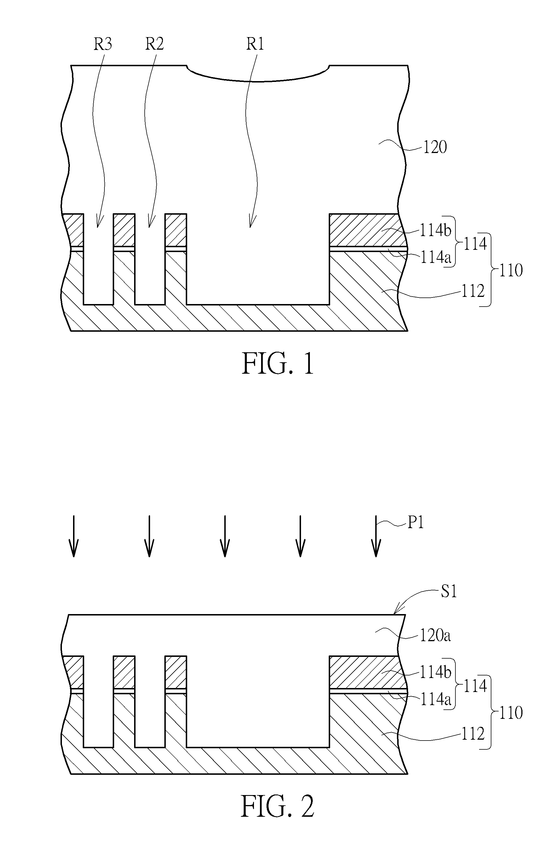
[0014]FIGS. 1-4 schematically depict cross-sectional views of a semiconductor process according to the present invention. As shown in FIG. 1, a substrate 110 is provided. The substrate 110 may include a bulk substrate 112 and a layer 114. The bulk substrate 112 may be a semiconductor substrate such as a silicon substrate, a silicon containing substrate, a III-V group-on-silicon (such as GaN-on-silicon) substrate, a graphene-on-silicon substrate or a silicon-on-insulator (SOI) substrate. The layer 114 may be a single layer or multi-layers according to the needs. In this embodiment, the layer 114 includes an oxide layer 114a and a nitride layer 114b from bottom to top; in another embodiment, the layer 114 may be an oxide layer or a nitride layer or similar.

[0015]More precisely, the substrate 110 has trenches R1, R2, R3 and the layer 114 covers the bulk substrate 112 other than the trenches R1, R2, R3. In this embodiment, the layer 114 serves as a hard mask for etching the bulk substra...

second embodiment

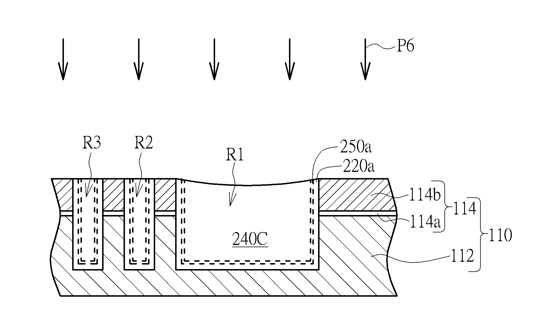
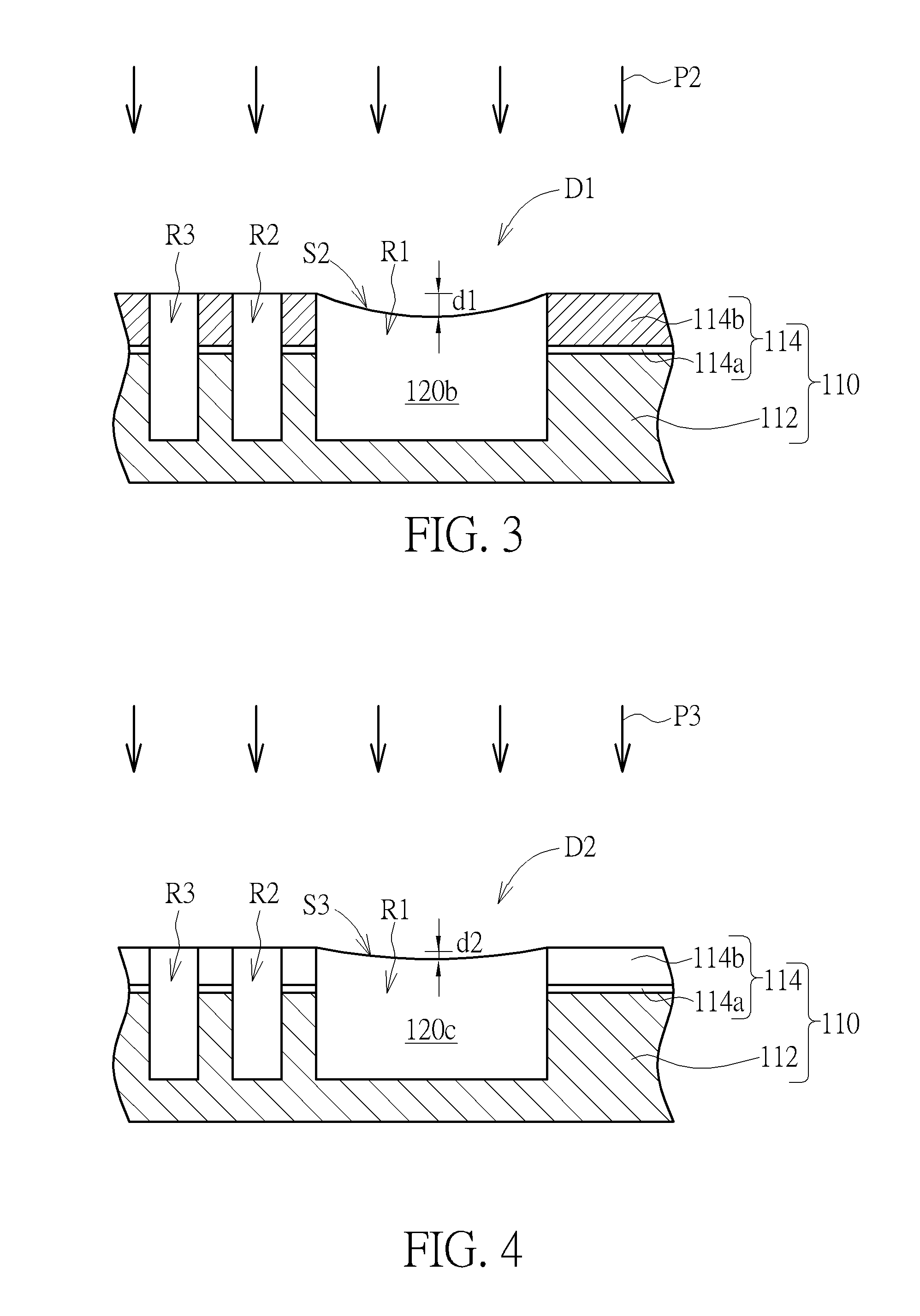
[0020]Accordingly, the dishing D1 caused by polishing the oxide layer 120a in the trenches R1, R2, R3 with different sizes can be reduced. However, the loss of the nitride layer 114b, is high, and the depth d3 of the oxide layer 120c is reduced, that would degrade a formed semiconductor structure. For instance, as the oxide layer 120c is applied to serve as an isolation structure, the performance degrades due to the lost and the shortening of the oxide layer 120c. Therefore, a second embodiment is provided as follows to solve the problem.

[0021]FIGS. 5-8 schematically depict cross-sectional views of a semiconductor process according to a second embodiment of the present invention. As shown in FIG. 5, a substrate 110 is provided. The substrate 110 may a bulk substrate 112 and a layer 114. The bulk substrate 112 may be a semiconductor substrate such as a silicon substrate, a silicon containing substrate, a III-V group-on-silicon (such as GaN-on-silicon) substrate, a graphene-on-silicon...


PUM


Abstract

A semiconductor process includes the following steps. A substrate having trenches with different sizes is provided. A first oxide layer is formed to entirely cover the substrate. A prevention layer is formed on the first oxide layer. A first filling layer is formed on the prevention layer and fills the trenches until the first filling layer is higher than the substrate. A first polishing process is performed to polish the first filling layer until exposing the prevention layer. A second polishing process is performed to polish the first filling layer, the prevention layer and the first oxide layer until the substrate is exposed.

Description

BACKGROUND OF THE INVENTION[0001]1. Field of the Invention[0002]The present invention relates generally to a semiconductor process, and more specifically to a semiconductor process that applies chemical mechanical polishing (CMP) processes.[0003]2. Description of the Prior Art[0004]In the semiconductor industry, chemical mechanical polishing (CMP) is the most common and important planarization tool applied. Generally, the CMP process can be used to remove a topographical target of a thin film layer on a semiconductor wafer and to produce a wafer with both a regular and planar surface. In a CMP process, slurry is provided in a surface subject to planarization, and a mechanical polishing process is performed on the surface of the wafer. The slurry includes chemical agents and abrasives. The chemical agents may be PH buffers, oxidants, surfactants or the like, and the abrasives may be silica, alumina, zirconium oxide, or the like. The chemical reactions evoked by the chemical agents an...

Claims


Application Information

Patent Timeline
IPC IPC(8): H01L21/3105H01L21/762
CPCH01L21/76224H01L21/31053
Inventor HUANG, PO-CHENGLI, YU-TINGWANG, CHUN-HSIUNGSIE, WU-SIANLIU, YI-LIANGHSU, CHIA-LINTSENG, I-MING
Owner UNITED MICROELECTRONICS CORP
Why Eureka
Try Eureka