Plasma enhanced vapor phase deposition

US20150147488A1Inactive Publication Date: 2015-05-28SK HYNIX INC +1

Image

  • Plasma enhanced vapor phase deposition
  • Plasma enhanced vapor phase deposition
  • Plasma enhanced vapor phase deposition

Examples


Embodiment Construction

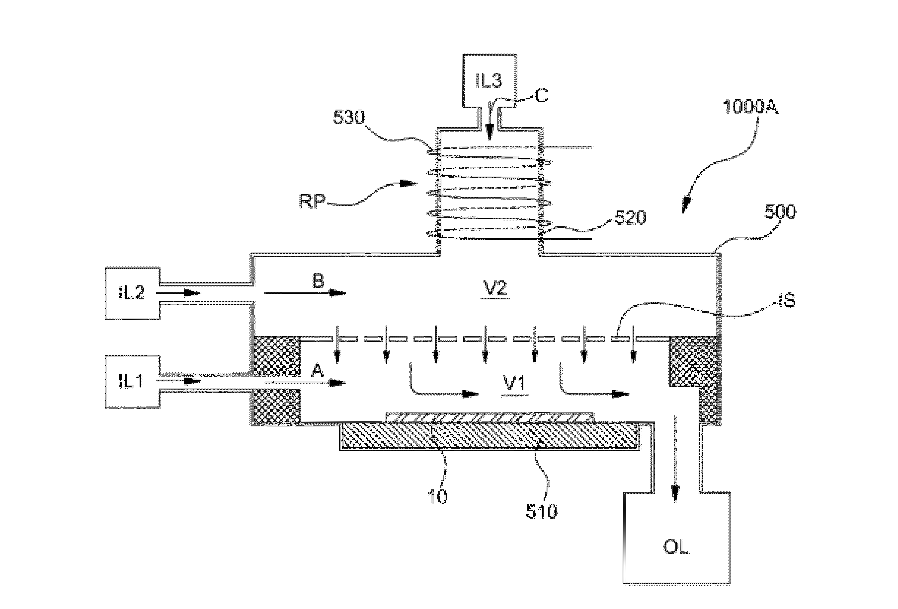
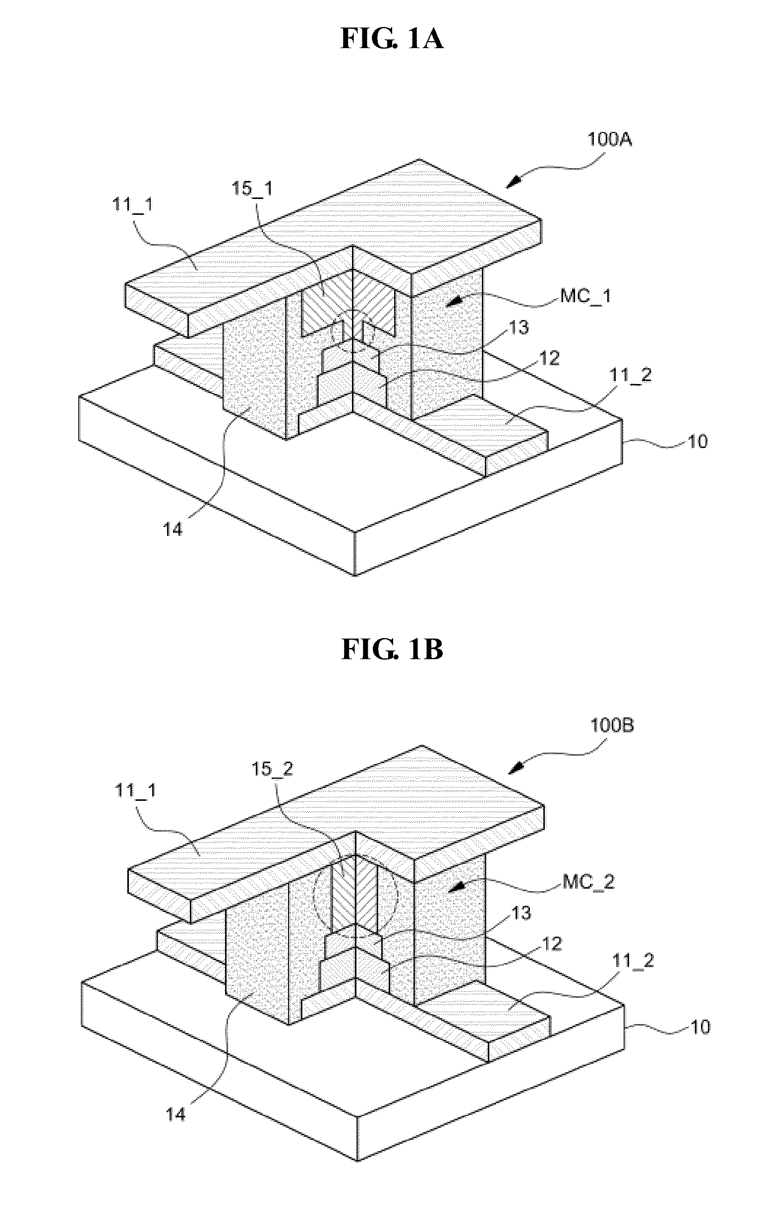
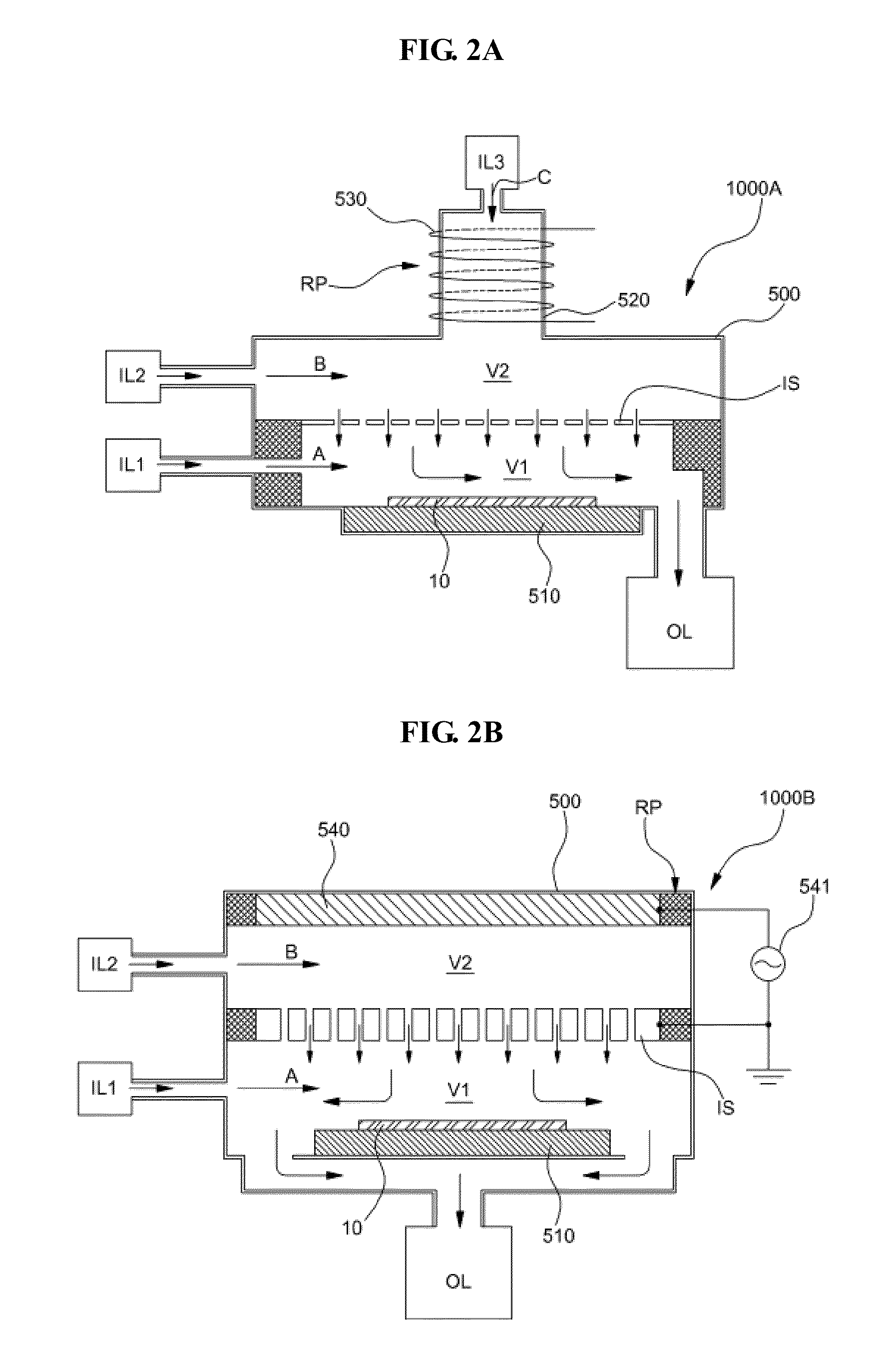
[0034]The present invention will now be described more fully with reference to the accompanying drawings, in which exemplary embodiments of the invention are shown.

[0035]The invention may, however, be embodied in many different forms and should not be construed as being limited to the embodiments set forth herein; rather these embodiments are provided so that this disclosure will be thorough and complete, and will fully convey the concept of the invention to one of ordinary skill in the art.

[0036]The same reference numerals denote the same elements in the drawings. As used herein, the term “and / or” includes any and all combinations of one or more of the associated listed items.

[0037]The terminology used herein is for the purpose of describing particular embodiments only and is not intended to be limiting of exemplary embodiments. As used herein, the singular forms “a,”“an” and “the” are intended to include the plural forms as well, unless the context clearly indicates otherwise. It ...


PUM

PropertyMeasurementUnit
Temperatureaaaaaaaaaa
Widthaaaaaaaaaa
Widthaaaaaaaaaa

Abstract

A plasma enhanced vapor deposition apparatus includes a process chamber including a first space and a second space, a substrate holder provided in the first space and supporting a substrate, a plasma generating device combined to the process chamber and inducing plasma in the second space, an ion species screening member separating the first and second spaces from each other and filtering ion species to prevent the ion species from diffusing from the second space to the first space, a first gas supplier supplying a first process gas including a precursor gas into the first space, wherein the precursor gas includes atoms constituting a material layer deposited over the substrate, a second gas supplier supplying a second process gas including a reactive gas into the second space, and a gas discharger coupled to the process chamber and inducing a gas flow from the second space to the first space.

Description

CROSS-REFERENCES TO RELATED APPLICATION[0001]This application claims the benefit of Korean Patent Application No. 10-2013-0144926, filed on Nov. 26, 2013, in the Korean Intellectual Property Office, the disclosure of which is incorporated herein in its entirety by reference.BACKGROUND[0002]1. Field of the Invention[0003]The present invention relates to a technique for fabricating semiconductor device, and more particularly, to a plasma enhanced vapor deposition apparatus for depositing a non-volatile data storing film, a plasma enhanced vapor deposition method, and a computer readable recording medium.[0004]2. Description of the Related Art[0005]Due to recent increases in demands for portable digital application devices, such as smart phones, tablet PCs, and digital cameras, the non-volatile memory market is rapidly growing. An example of programmable non-volatile memory devices is a flash memory. Since a 16 kb EEPROM was introduced in 1983, flash memories have been continuously sca...

Claims


Application Information

Patent Timeline
28 May 2015
Publication
US20150147488A1
IPC
C23C16/50; C23C16/455; C23C16/458
CPC
C23C16/50; C23C16/458; C23C16/45565; C23C16/455; C23C16/45523; C23C16/305; C23C16/452; C23C16/505
Inventors
CHOI, DOO JIN; JEONG, JIN HWAN