Methods of operating bonding machines for bonding semiconductor elements, and bonding machines

Active Publication Date: 2015-06-18
KULICKE & SOFFA IND INC
View PDF27 Cites 35 Cited by
  • Summary
  • Abstract
  • Description
  • Claims
  • Application Information

AI Technical Summary

Problems solved by technology

Through the cyclical application of heat (e.g., through the heater in the bond head assembly), and through changes to th

Method used


Image

  • Methods of operating bonding machines for bonding semiconductor elements, and bonding machines
  • Methods of operating bonding machines for bonding semiconductor elements, and bonding machines
  • Methods of operating bonding machines for bonding semiconductor elements, and bonding machines

Examples


Embodiment Construction

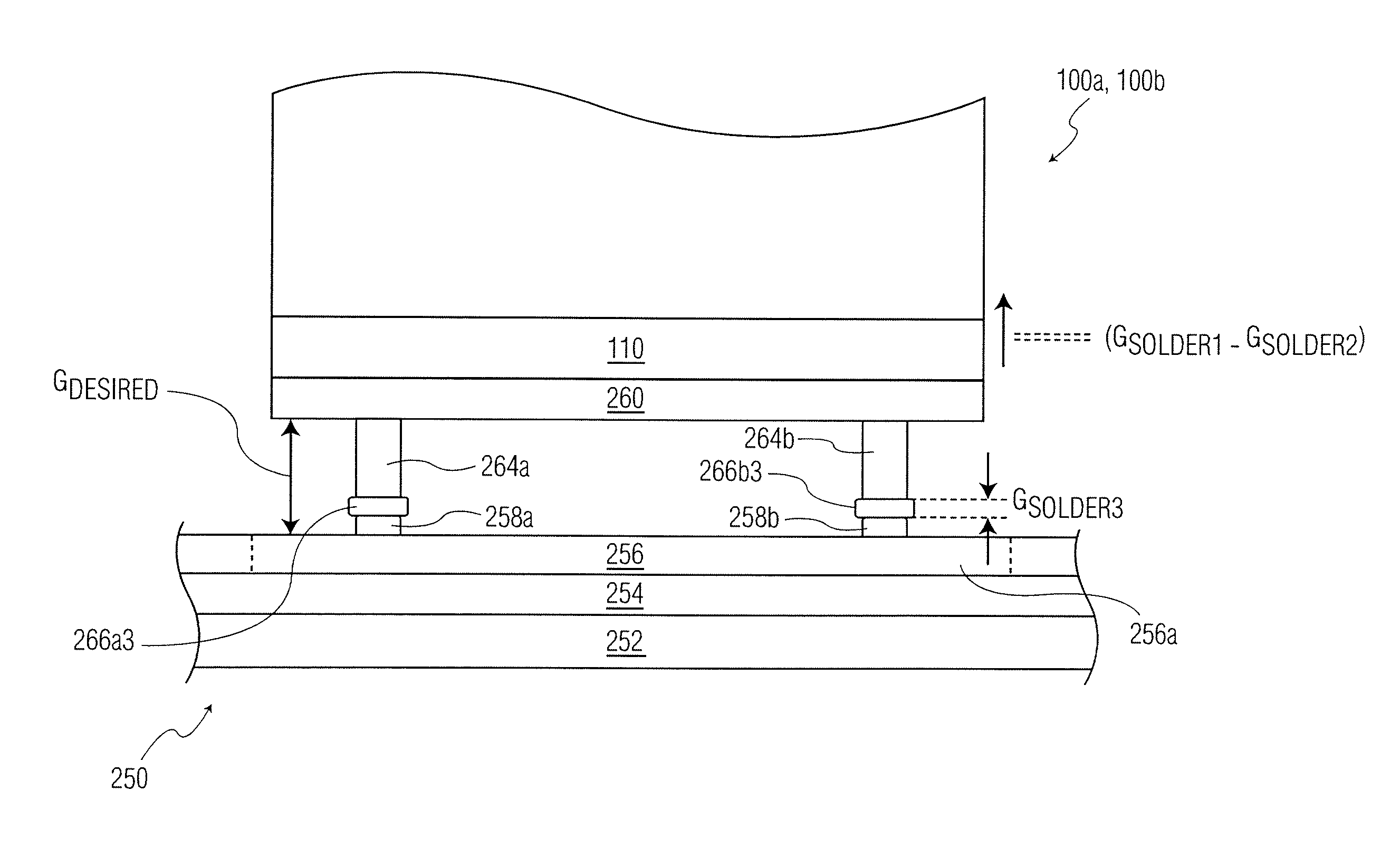
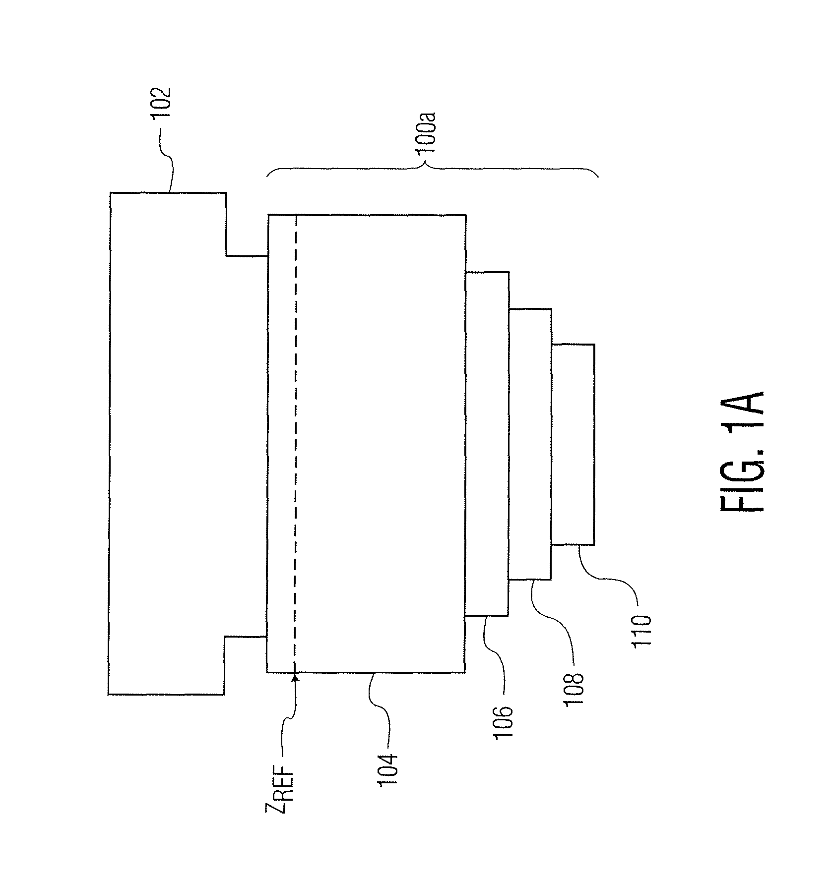
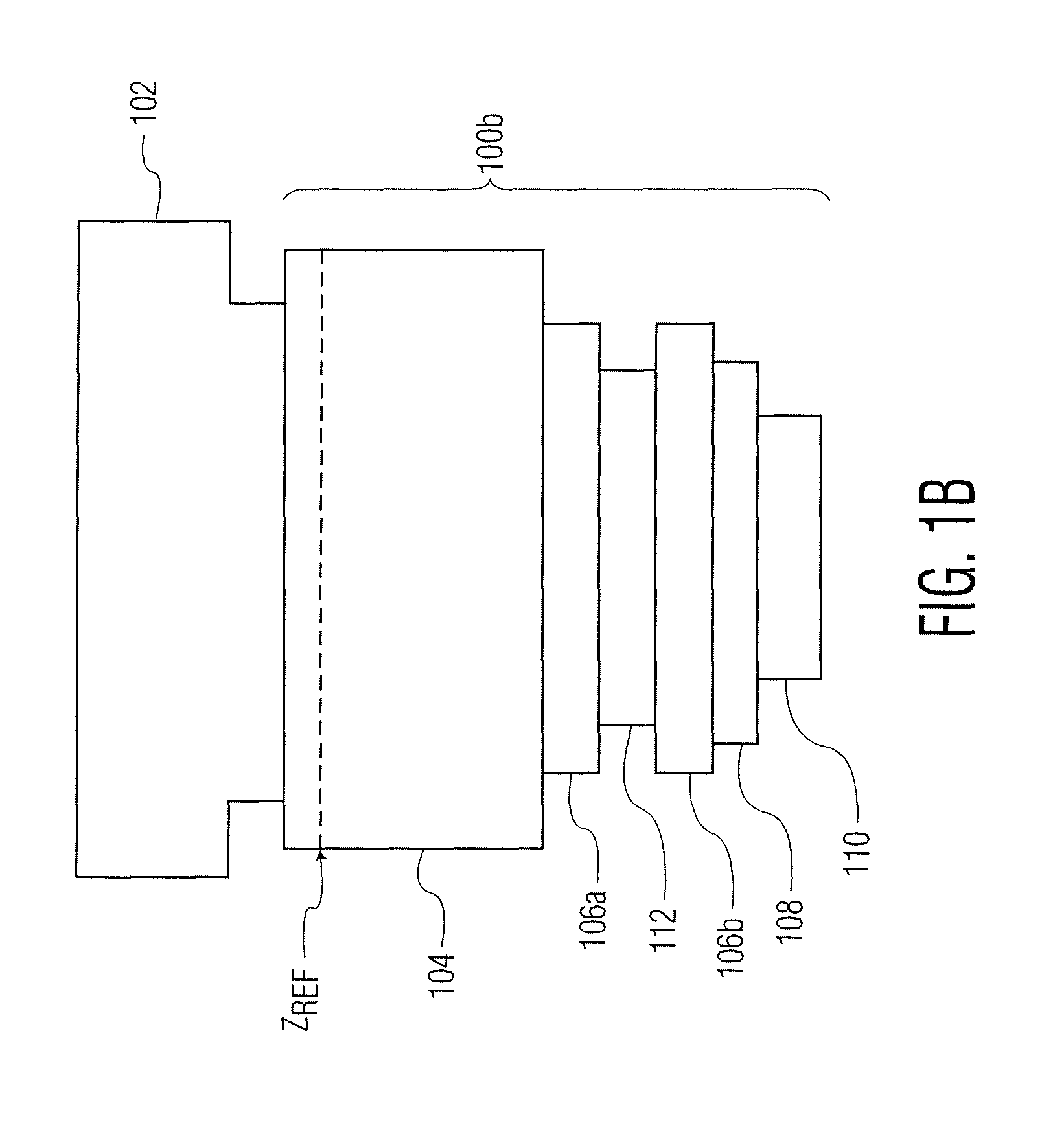
[0018]As used herein, the term “semiconductor element” is intended to refer to any structure including (or configured to include at a later step) a semiconductor chip or die. Exemplary semiconductor elements include a bare semiconductor die, a semiconductor die on a substrate (e.g., a leadframe, a PCB, a carrier, a semiconductor chip, a semiconductor wafer, a BGA substrate, a semiconductor element, etc.), a packaged semiconductor device, a flip chip semiconductor device, a die embedded in a substrate, a stack of semiconductor die, amongst others. Further, the semiconductor element may include an element configured to be bonded or otherwise included in a semiconductor package (e.g., a spacer to be bonded in a stacked die configuration, a substrate, etc.).

[0019]As used herein, the term “substrate” is intended to refer to any structure to which a semiconductor element may be bonded (e.g., thermocompressively bonded, ultrasonically bonded, thermosonically bonded, die bonded, etc.). Exem...


PUM

PropertyMeasurementUnit
Temperatureaaaaaaaaaa
Timeaaaaaaaaaa
Forceaaaaaaaaaa

Abstract

A method of operating a bonding machine for bonding semiconductor elements is provided. The method includes the steps of: (a) measuring a time based z-axis height measurement characteristic of a bond head assembly during a model bonding process; (b) determining a z-axis adjustment profile for a subsequent bonding process based on the measured time based z-axis height measurement characteristic; and (c) adjusting a z-axis position of the bond head assembly with a z-axis motion system during the subsequent bonding process using the z-axis adjustment profile.

Description

CROSS REFERENCE TO RELATED APPLICATION[0001]This application claims the benefit of U.S. Provisional Patent Application No. 61 / 916,912 filed Dec. 17, 2013, the content of which is incorporated herein by reference.FIELD OF THE INVENTION[0002]The present invention relates to the formation of semiconductor packages, and more particularly, to improved methods of operating bonding machines for bonding semiconductor elements.BACKGROUND OF THE INVENTION[0003]In certain aspects of the semiconductor packaging industry, semiconductor elements are bonded to bonding locations. For example, in conventional die attach (also known as die bonding) applications, a semiconductor die is bonded to a bonding location of a substrate (e.g., a leadframe, another die in stacked die applications, a spacer, etc.). In advanced packaging applications, semiconductor elements (e.g., bare semiconductor die, packaged semiconductor die, etc.) are bonded to bonding locations of a substrate (e.g., a leadframe, a PCB, a...

Claims


Application Information

Patent Timeline
IPC IPC(8): H01L23/00B23K31/12H01L21/66B23K1/00
CPCH01L24/75B23K1/0016B23K31/12H01L22/10H01L24/81H01L2224/75901H01L2224/81201H01L2224/81986H01L2224/75001H01L2224/75252H01L2224/75301H01L2224/81121H01L24/13H01L2224/131H01L2224/13147H01L2224/81203H01L2224/7592H01L2224/75842H01L2224/75841H01L2224/75702H01L2224/81815H01L2924/00012H01L2924/00014H01L2924/014H05K3/34H01L21/00B23K3/00B23K3/04B23K3/08H01L2224/81801
Inventor WASSERMAN, MATTHEW B.SCHMIDT-LANGE, MICHAEL P.COLOSIMO, JR., THOMAS J.
Owner KULICKE & SOFFA IND INC
Why Eureka
Try Eureka