Electronic packaged device and manufacturing method thereof

a technology of electronic packaging and packaging layers, applied in the direction of electrical apparatus casings/cabinets/drawers, conductive pattern formation, earth/grounding circuits, etc., can solve the problems of increasing the difficulty of designing the electromagnetic shielding layer in electronic packaging, and the frequency of electromagnetic interference between different electronic components, so as to prevent electromagnetic interference

Active Publication Date: 2015-06-18
UNIVERSAL SCIENTIFIC INDUSTRIAL (SHANGHAI) CO LTD
View PDF4 Cites 19 Cited by
  • Summary
  • Abstract
  • Description
  • Claims
  • Application Information

AI Technical Summary

Benefits of technology

[0008]An embodiment of the instant disclosure provide an electronic packaging device which includes a shielding structure for prevent electromagnetic interferences between electronic components.
[0012]In summary, the instant disclosure provides a manufacturing method of package device, in which electronic components are fixed onto a substrate carrier, and an encapsulating member is disposed on the surface of the substrate carrier to cover the electronic components. The substrate carrier is then separated from the encapsulating member. First trench is then formed on a first surface of the encapsulating member. Conductive material is disposed on the first surface of the encapsulating member and the outer surface of the first trench to form a conductive layer. The conductive layer is patterned to form a circuit layer, so that the circuit layer is formed directly on the encapsulating member instead of a circuit board to reduce the volume of the packaging. Successively, second trench is formed on the second surface of the encapsulating member. The second trench and the first trench are interconnected. A shielding structure is then formed in the first and the second trenches to reduce the electromagnetic and radio frequency interferences between encapsulating compartments. An electromagnetic shielding layer is then formed and is electrically connected to grounding pads.
[0013]The electronic packaged device of the instant disclosure includes an encapsulating member and a shielding structure. The shielding structure is interposed between different encapsulating compartments to reduce the electromagnetic and radio frequency interferences between encapsulating compartments. The shielding structure can transmit electromagnetic interfering signals to the surrounding via grounding pads, and enhance the effects of electromagnetic shielding for the electronic packaged device.

Problems solved by technology

Accordingly, electromagnetic interferences between different electronic components occur more often than ever.
As a result, designing electromagnetic shielding layer in electronic packaging is becoming relatively more difficult.

Method used


Image

  • Electronic packaged device and manufacturing method thereof
  • Electronic packaged device and manufacturing method thereof
  • Electronic packaged device and manufacturing method thereof

Examples


first embodiment

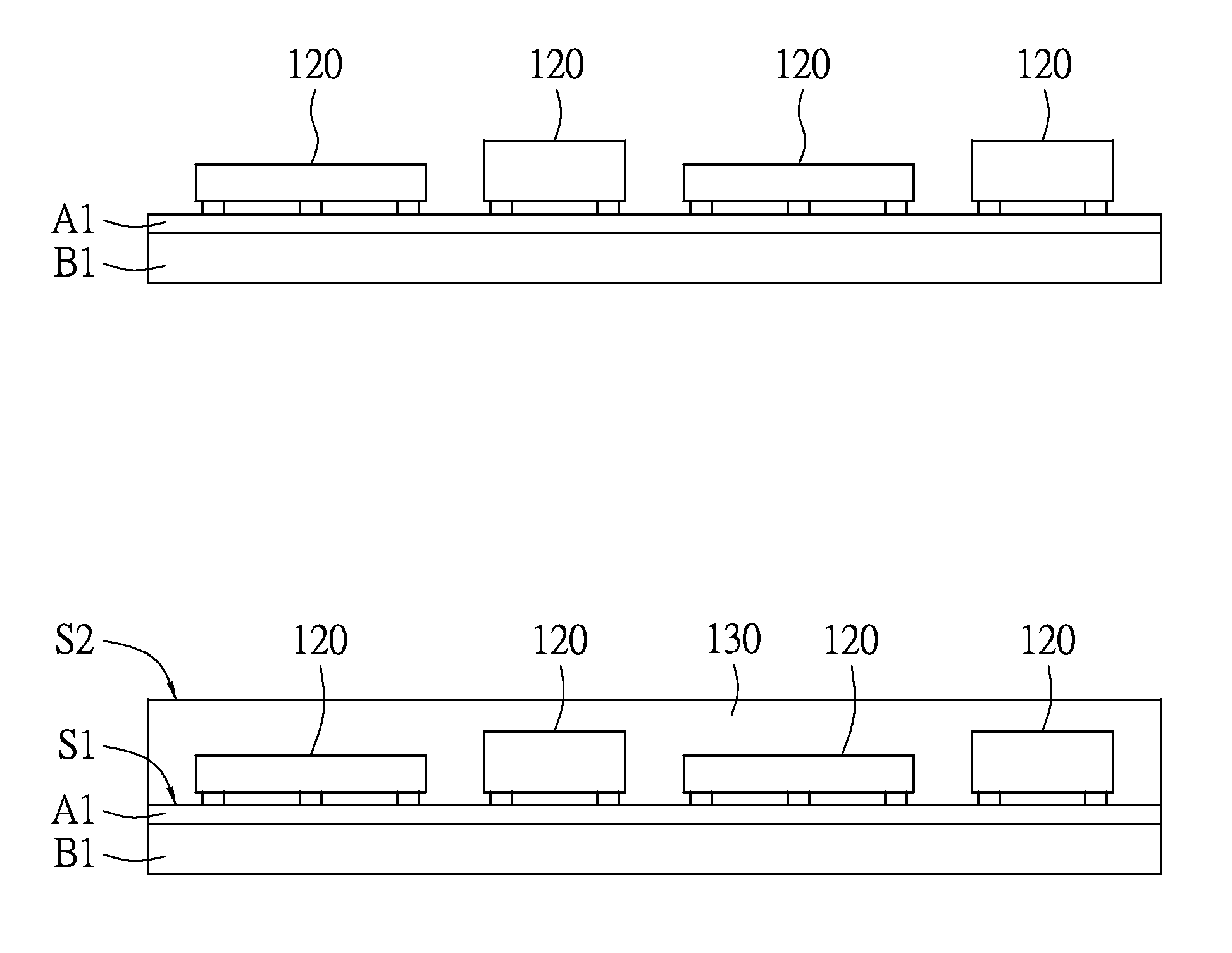
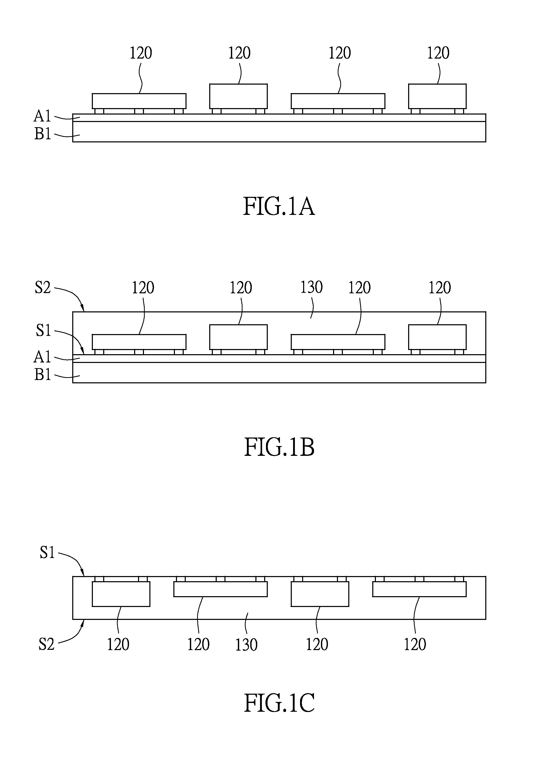
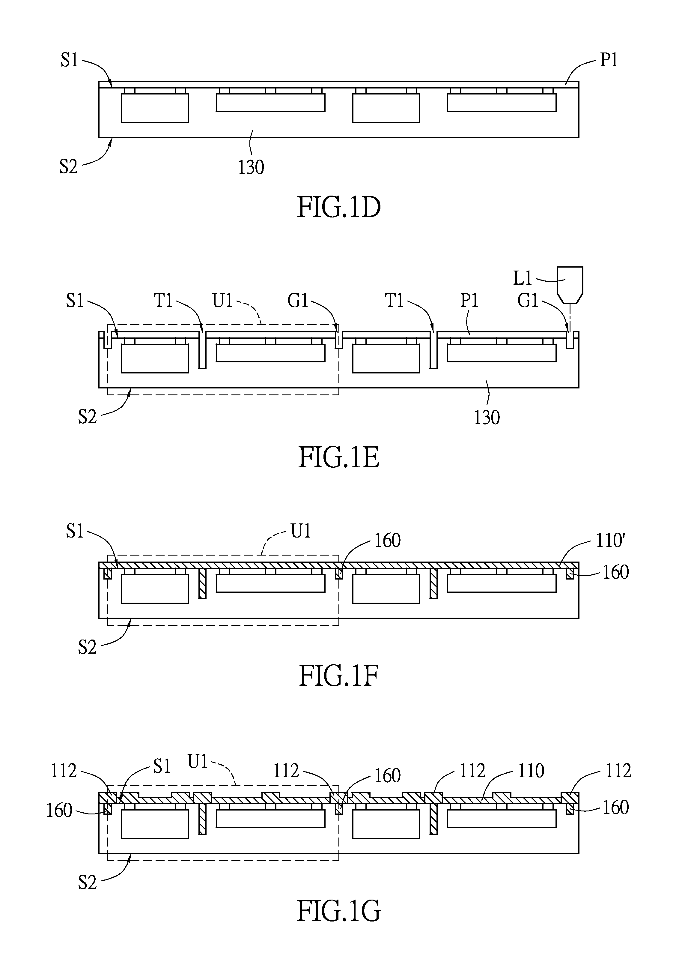
[0019]Please refer to FIGS. 1A to 1K as schematic diagrams illustrating steps of an electronic packaged device manufacturing method in accordance with the instant disclosure.

[0020]As shown in FIG. 1A, a plurality of electronic components 120 is configured on a surface of a substrate carrier B1. Adhesives A1 are applied onto the surface of the substrate carrier B1 to fix the electronic components 120 on the substrate carrier B1. Notably, the electronic components 120 can be chips, transistors, diodes, capacitors, inductors, or the like. The adhesives A1 can be glue, double sided tape, adhesive inks or the like. However, the coupling between the electronic components 120 and the substrate carrier B1 is not limited to the examples provided herein.

[0021]Please refer to FIG. 1B. An encapsulating member 130 is disposed on the surface of the substrate carrier to cover the electronic components 120. Typically, the encapsulating member 130 can be molding sealant or prepreg adhesives. The enc...

second embodiment

[0055]Please refer to FIG. 2C as schematic diagrams illustrating the structure of the electronic packaged device in accordance with the instant disclosure. The electronic packaged device 200 and the electronic packaged device 100 are similar, so the differences will be disclosed as follow.

[0056]In the instant embodiment, the shielding structure 240 is formed by spray coating, sputtering, printing, injection or the like to fill the trench F1 with conductive material. The shielding structure 240 extends from the first surface S1 (bottom surface) to the second surface S2 (top surface) of the encapsulating member 130 and is electrically connected to the electromagnetic shielding layer 150.

[0057]Moreover, the electromagnetic shielding layer 150 covers the second surface S2 of the encapsulating member 130 to electrically connect to the shielding structure 240, and the electromagnetic shielding layer 150 is physically and electrically connected to the grounding structure 260 at the sides o...


PUM

PropertyMeasurementUnit
diametersaaaaaaaaaa
conductiveaaaaaaaaaa
electromagneticaaaaaaaaaa

Abstract

A manufacturing method of electronic packaged device includes the following. A plurality of electronic components is disposed on a substrate carrier. An encapsulating member is disposed on the substrate carrier and covers the electronic components. The substrate carrier is separated from the encapsulating member. A plurality of first trenches is arranged on a first surface of the encapsulating member. Conductive material is disposed onto the first surface and into the first trenches to form a conductive layer. The conductive layer is patterned on the first surface to form a circuit layer. The circuit layer includes at least one grounding pad. A plurality of second trenches is arranged on a second surface of the encapsulating member. At least one shielding structure is formed in the first trenches and the second trenches. An electromagnetic shielding layer is connected to the grounding pad.

Description

BACKGROUND OF THE INVENTION[0001]1. Field of the Invention[0002]The instant disclosure relates to an electronic packaged device and the manufacturing method thereof.[0003]2. Description of Related Art[0004]Most electronic packaging devices use a variety of packaging materials to package electronic components. Since electronic products have more and more functions, thus the electronic components in the electronic packaging devices corresponding increases as well. Accordingly, electromagnetic interferences between different electronic components occur more often than ever.[0005]Typically, in order to reduce various electromagnetic interference and radio frequency interferences generated by electronic components, an electromagnetic interference (EMI) layer is designed in the electronic packaging to isolate different electronic components. Alternatively, an external metal cover (Metal lid) is installed on the electronic packaging.[0006]However, in the climate of miniaturization, the ove...

Claims


Application Information

Patent Timeline
Patent Type & Authority Applications(United States)
IPC IPC(8): H05K13/04H05K9/00
CPCH05K9/0032H05K13/046H05K9/0037H05K9/0039H01L21/568H01L24/19H01L24/96H01L24/97H01L2924/1815H01L2924/3025H01L2224/04105Y10T29/49155H05K1/181H05K9/0022H05K9/0064H05K2201/09036H05K2201/10371
Inventor CHEN, JEN-CHUNSHIH, PAI-SHENG
Owner UNIVERSAL SCIENTIFIC INDUSTRIAL (SHANGHAI) CO LTD
Why Eureka
Try Eureka