Method of cutting high-hardness material with multi-wire saw

Inactive Publication Date: 2015-07-23
HITACHI METALS LTD
View PDF3 Cites 13 Cited by
  • Summary
  • Abstract
  • Description
  • Claims
  • Application Information

AI Technical Summary

Benefits of technology

The present invention provides a method for cutting high-hardness materials with a multi-wire saw that improves machining accuracy. By repeatedly making a run cycle in which the wire is moved back and forth to a continuous travel distance that is 20 times or more as long as the maximum total contact length between a given ingot and the wire, the work of the wire in contact with the ingot can be both reduced and averaged compared to conventional techniques. This reduces the waving or warp of multiple wafers to be sliced off from the ingot. Additionally, by setting the length of the wire newly fed in a run cycle to be 0.35 to 1.55 times as large as the maximum total contact length, the wire can be kept sharp enough for a long time. Furthermore, wire snapping can be minimized while the ingot is being cut.

Problems solved by technology

However, compared to silicon wafers which are currently being mass-produced and used extensively, it is far more difficult to cut such a high-hardness material with high machining accuracy and finish it into a wafer with a high degree of planarity.

Method used


Image

  • Method of cutting high-hardness material with multi-wire saw
  • Method of cutting high-hardness material with multi-wire saw
  • Method of cutting high-hardness material with multi-wire saw

Examples


examples

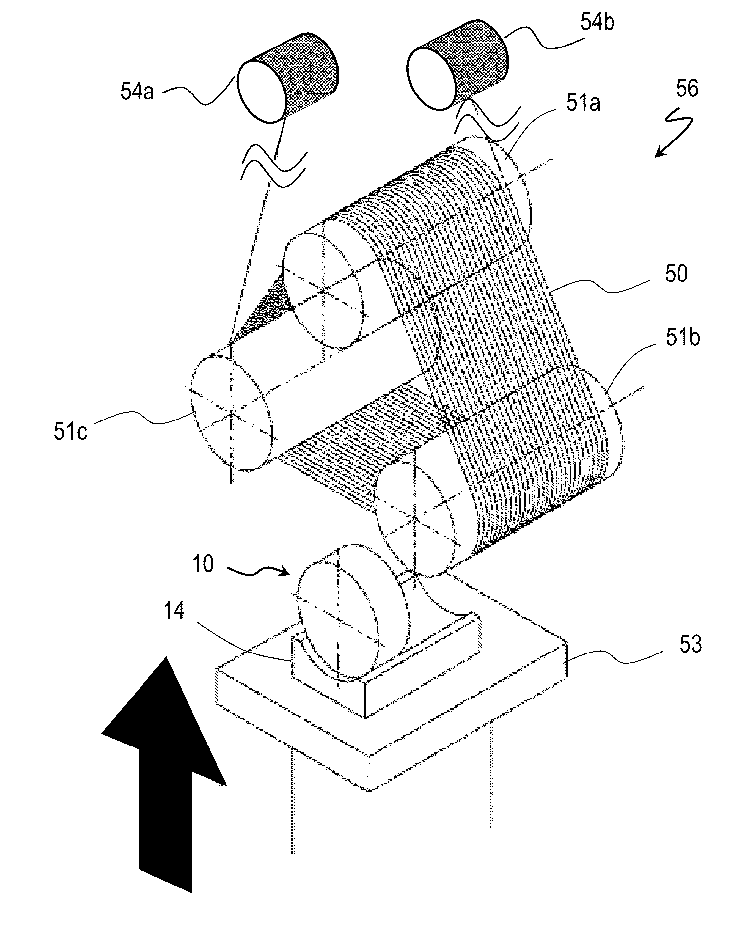
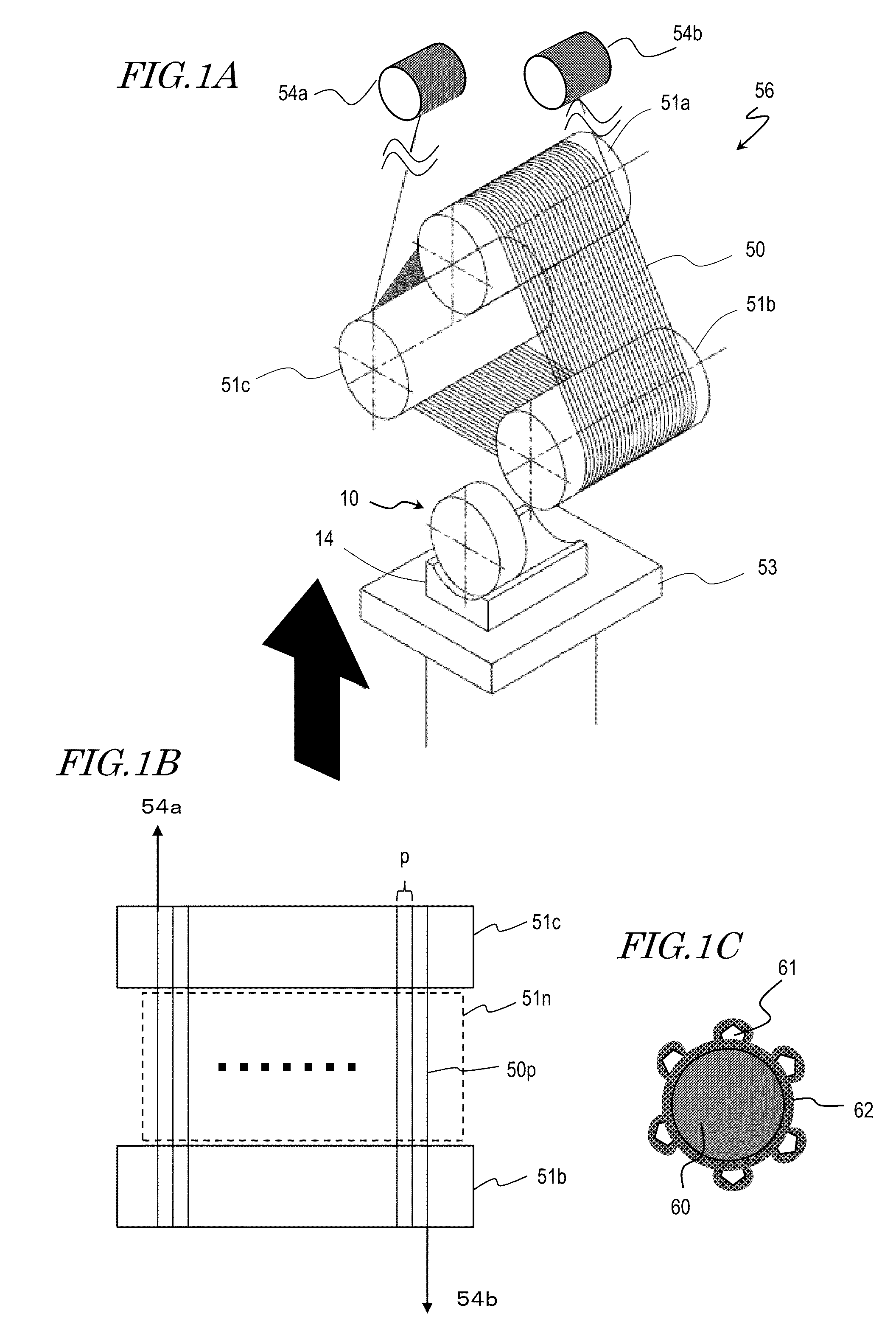
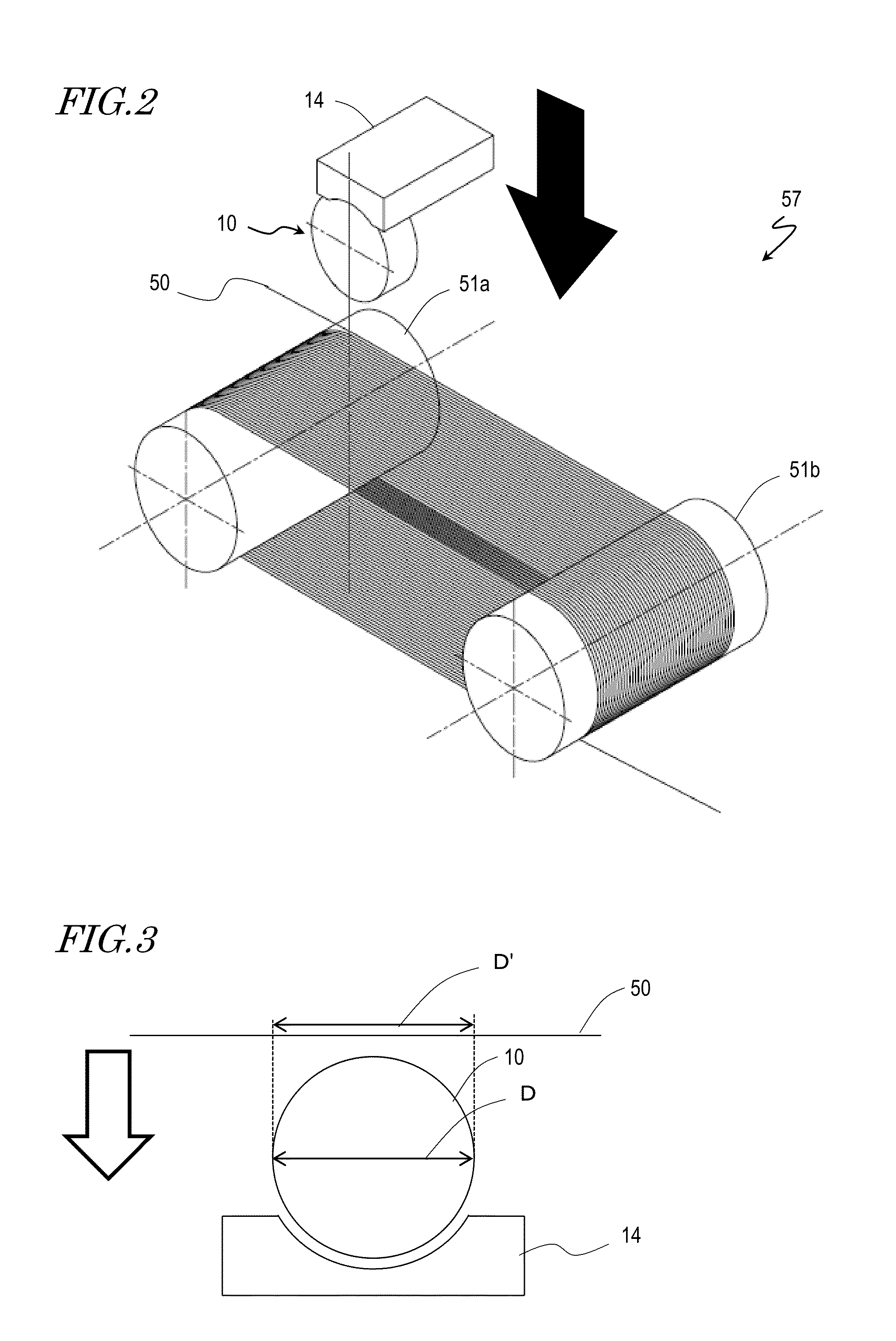
[0073]The present inventors carried out some experimental examples in which an ingot of a high-hardness material was sliced by the cutting method of this embodiment to find how much warp the wafers thus sliced off had. The results will be described below.

[0074]As an ingot of a high-hardness material, an ingot of single crystal sapphire in the shape of a circular cylinder with a diameter of 150 mm (i.e., 6 inches) was provided so as to slice off wafers, of which the principal surface was an r-plane. The ingot was cut using the following multi-wire saw, abrasive-particle-fixed wire and abrasive slurry:

[0075]Multi-wire saw: multi-wire saw MWS-34 produced by Takatori Corporation;[0076]Wire: diamond-electrodeposited wire produced by Allied Material (A. L. M. T. Corp.) and having a wire diameter of 180 μm and an average abrasive particle size of 35 μm; and[0077]Abrasive Slurry: DKW-2 produced by Allied Material (A. L. M. T. Corp.)

[0078]The ingot was sliced into wafers representing Example...


PUM

PropertyMeasurementUnit
Lattice constantaaaaaaaaaa
Lengthaaaaaaaaaa
Abrasiveaaaaaaaaaa

Abstract

In a method of cutting a high-hardness material with a multi-wire saw, an ingot of the high-hardness material is sliced into a plurality of wafers by cutting the ingot at multiple points simultaneously with the multi-wire saw. The method comprises repeating a run cycle of reciprocating motion of a wire of the multi-wire saw so that the relationships (1) c1≧20, given C1=b / a and (2) 0.35≦c2≦1.55, given c2=d / a are satisfied, where a is a maximum total contact length defined as a sum of the lengths of the ingot as projected onto multiple cut points when projecting the ingot onto the wire in a direction in which the ingot is going to be cut, b is a continuous travel distance of the wire, and d is a length of the wire newly fed in each said run cycle.

Description

BACKGROUND[0001]1. Technical Field[0002]The present disclosure relates to a method of cutting a high-hardness material with a multi-wire saw.[0003]2. Description of the Related Art[0004]Recently, silicon carbide semiconductors have attracted a lot of attention as a new type of semiconductor materials. Silicon carbide semiconductors have a greater dielectric breakdown voltage, a higher electron saturated drift velocity, and a higher thermal conductivity than silicon semiconductors. For that reason, researches and developments have been carried on extensively to realize, using those silicon carbide semiconductors, power devices which can operate at higher temperatures, at higher speeds and with a larger amount of current supplied than conventional silicon devices. Among other things, since motors for use in electric motorcycles, electric cars and hybrid cars are either AC driven or inverter-controlled, development of high-efficiency switching elements for use in those applications is ...

Claims


Application Information

Patent Timeline
IPC IPC(8): B23D61/18B28D1/08
CPCB28D1/08B23D61/185B28D5/045
Inventor KONDO, SADAHIKOMIYACHI, AKIRA
Owner HITACHI METALS LTD
Why Eureka
Try Eureka