Semiconductor device

a technology of semiconductor devices and insulators, which is applied in the direction of semiconductor devices, diodes, electrical apparatus, etc., can solve the problems of reducing the withstand voltage of the semiconductor device, and achieve the effect of preventing local electric field concentration, and preventing the withstand voltage from decreasing

Inactive Publication Date: 2015-07-23
TOYOTA JIDOSHA KK
View PDF3 Cites 24 Cited by
  • Summary
  • Abstract
  • Description
  • Claims
  • Application Information

AI Technical Summary

Benefits of technology

[0006]In such a configuration, the first gate trenches and the second gate trenches are not in contact with each other such that there is no portion in which the first gate trenches and the second gate trenches intersect each other. This configuration makes it possible to prevent the trenches from becoming locally deeper due to the first gate trenches and the second gate trenches intersecting each other. This in turn makes it possible to prevent local electric field concentration, thus preventing a decrease in the withstand voltage of the semiconductor device. Further, since the decrease in the withstand voltage can be prevented here, it is not necessary to form p-type deep semiconductor region between adjoining gate trenches to obtain higher withstand voltage as in the technology of Patent Literature 1. Accordingly, no extra carriers (holes) are injected into diode region from the p-type semiconductor region such that annihilation time of carriers (holes) during reverse recovery of the diode can be shortened. This in turn makes it possible to inhibit switching loss during the reverse recovery. For the reasons stated above, the semiconductor device disclosed herein can have both the higher withstand voltage and the enhanced switching characteristics.

Problems solved by technology

This may undesirably cause electric field concentration near the deeper intersections and thus undesirably decrease the withstand voltage of the semiconductor device.

Method used


Image

  • Semiconductor device
  • Semiconductor device
  • Semiconductor device

Examples


Embodiment Construction

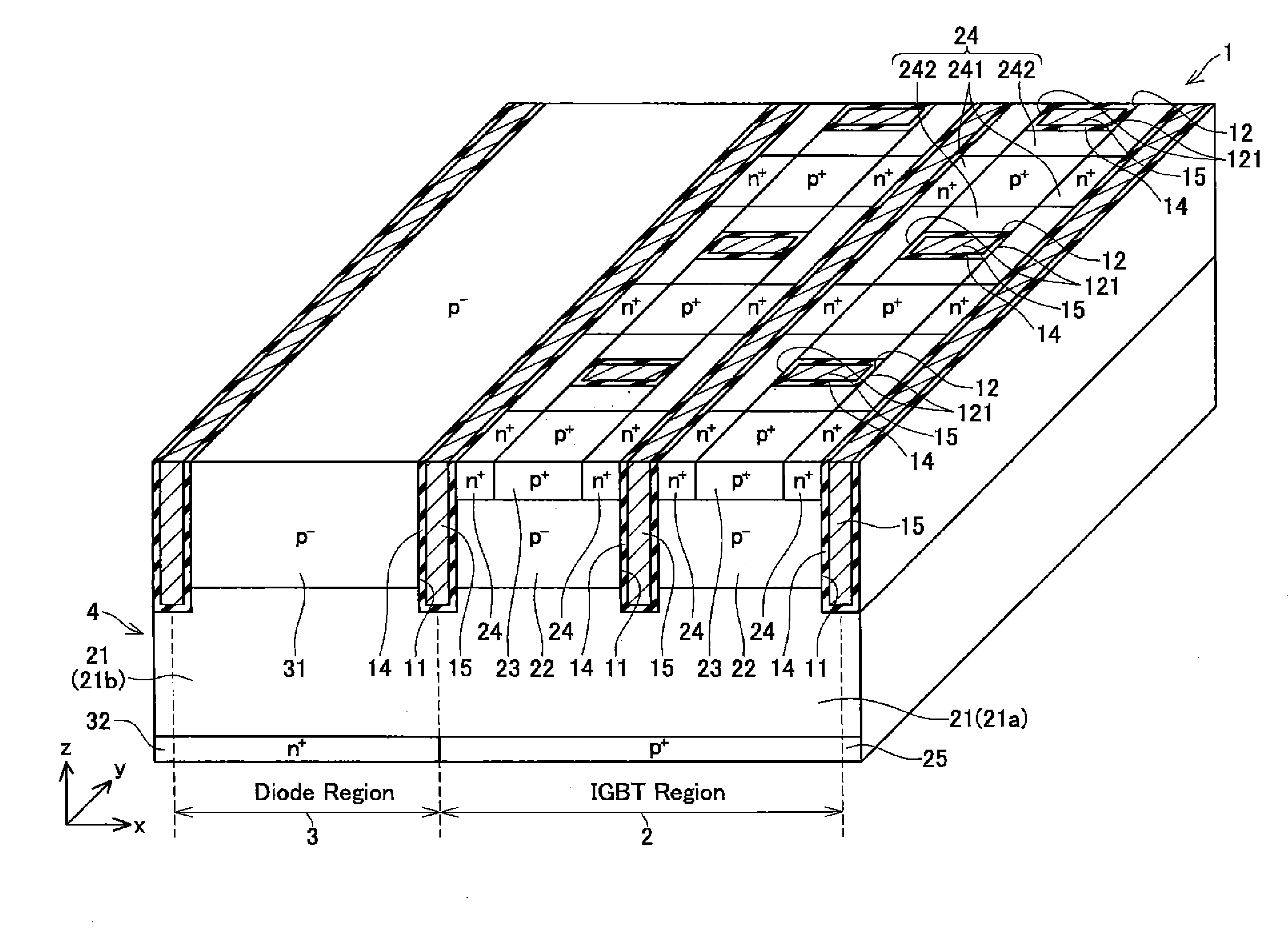
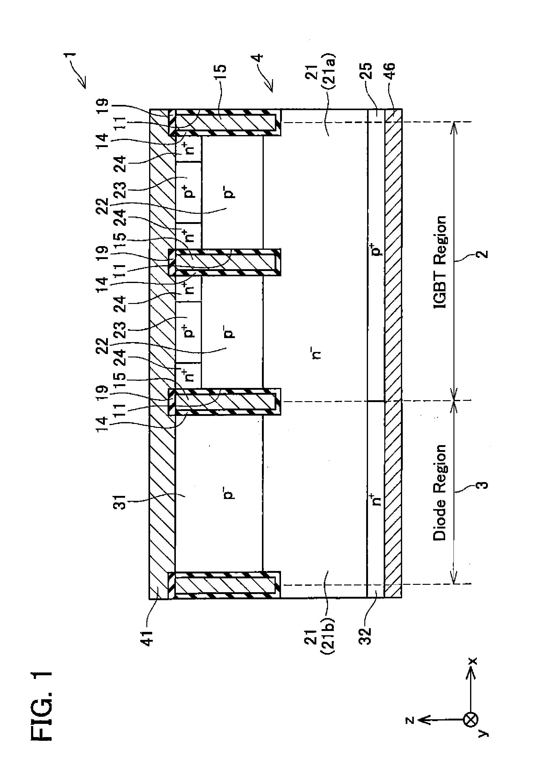
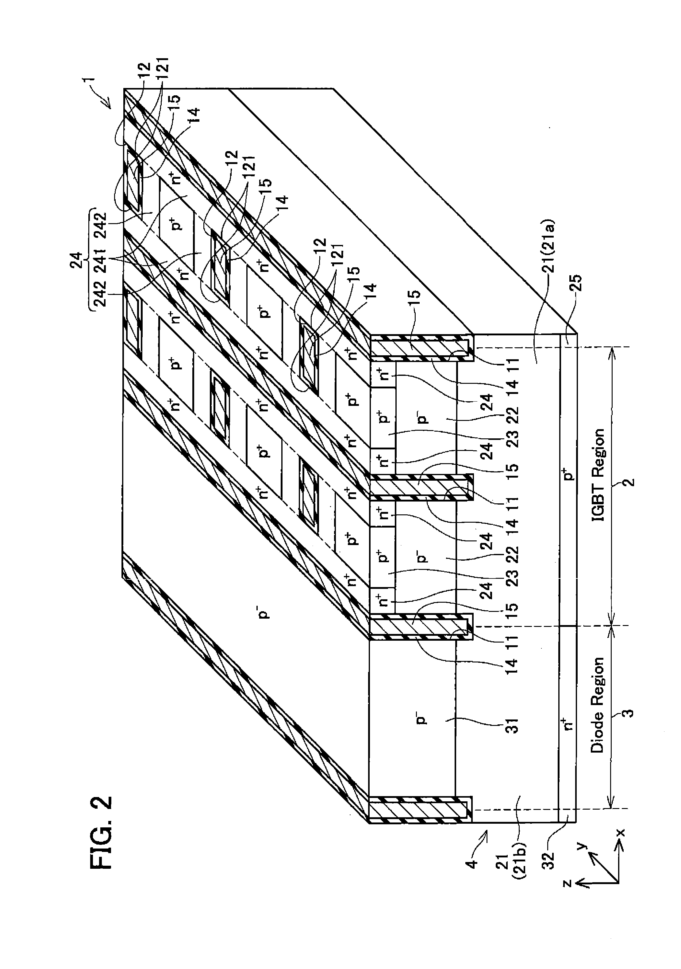
[0016]Embodiments are described below with reference to accompanying drawings. In the following description, hatching on some of configurations shown in the drawings is omitted for viewability of the drawings. A semiconductor device according to an embodiment is an RC-IGBT (Reverse Conducting Insulated Gate Bipolar Transistor) and has a function as an IGBT (Insulated Gate Bipolar Transistor) and a function as an FWD (Free Wheeling Diode). The IGBT and the FWD are arranged in a reverse-parallel state. As shown in FIGS. 1 and 2, a semiconductor device 1 includes a semiconductor substrate 4, an upper-surface-side common electrode 41 disposed on a upper surface side of the semiconductor substrate 4, and a lower-surface-side common electrode 46 disposed on a lower surface side of the semiconductor substrate 4 (Note that FIG. 2 omits to show the upper-surface-side common electrode 41 and the lower-surface-side common electrode 46.). Further, the semiconductor device 1 includes an IGBT reg...


PUM


Abstract

A semiconductor device 1 in which an IGBT region 2 and a diode region 3 adjoining each other are formed on a same substrate 4 is presented. The semiconductor device 1 is provided with a plurality of first gate trenches 11 extending abreast in a first direction in the IGBT region 2 and a plurality of second gate trenches 12 extending abreast in a second direction intersecting the first direction. The first gate trenches 11 and the second gate trenches 12 are not in contact with each other.

Description

CROSS-REFERENCE TO RELATED APPLICATION[0001]This application claims priority to Japanese Patent Application No. 2014-007713 filed on Jan. 20, 2014, the contents of which are hereby incorporated by reference into the present application.TECHNICAL FIELD[0002]A technology disclosed herein relates to a semiconductor device including gate trenches.DESCRIPTION OF RELATED ART[0003]Patent Literature 1 (Japanese Patent Application Publication No, 2003-529209) discloses a semiconductor device including a plurality of gate trenches. In the semiconductor device of Patent Literature 1, the plurality of gate trenches extends in directions intersecting each other. This semiconductor device includes a plurality of gate trenches extending in a longitudinal direction as viewed in planar view and a plurality of gate trenches extending in a transverse direction so as to orthogonally intersect the plurality of gate trenches extending in the longitudinal direction. A p-type deep semiconductor region is f...

Claims


Application Information

Patent Timeline
Patent Type & Authority Applications(United States)
IPC IPC(8): H01L29/739H01L29/423H01L27/06
CPCH01L29/7397H01L29/4236H01L27/0635H01L29/0696H01L27/0727
Inventor HIRABAYASHI, YASUHIROMACHIDA, SATORUYAMASHITA, YUSUKE
Owner TOYOTA JIDOSHA KK
Why Eureka
Try Eureka