Printing-based assembly of multi-junction, multi-terminal photovoltaic devices and related methods

Inactive Publication Date: 2015-07-23
THE BOARD OF TRUSTEES OF THE UNIV OF ILLINOIS +1
View PDF4 Cites 36 Cited by
  • Summary
  • Abstract
  • Description
  • Claims
  • Application Information

AI Technical Summary

Benefits of technology

[0009]The invention provides devices having multiple p-n junctions and corresponding terminals, including multi-junction, multi-terminal photovoltaic devices for the conversion of solar energy into electricity. In some embodiments, a multi-junction, multi-terminal device is combined with a single junction (1J) device or another multi-junction device in a stacked configuration via printing, such as dry contact transfer printing, to facilitate absorption of a wide range of wavelengths f

Problems solved by technology

Single junction (SJ) cells have a theoretical efficiency limit of ˜33.4% under one sun illumination, primarily due to the ineffective use of the entire solar spectrum.
To optimize the efficiency of SJ cells, multiple, separated SJ cells can be implemented with spectral-splitting optical elements to utilize more of the solar spectrum, but complexity in manufacturing, alignment and light management hinders use of such systems in practice.
This requirement becomes challenging to maintain as the number of

Method used


Image

  • Printing-based assembly of multi-junction, multi-terminal photovoltaic devices and related methods
  • Printing-based assembly of multi-junction, multi-terminal photovoltaic devices and related methods
  • Printing-based assembly of multi-junction, multi-terminal photovoltaic devices and related methods

Examples


example 1

Printing-Based Assembly of Quadruple Junction, Four-Terminal Microscale Solar Cells and Their use in High-Efficiency Modules

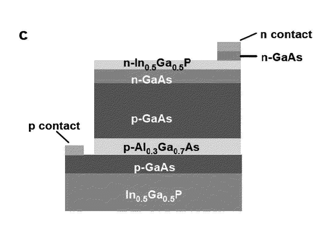
[0139]Expenses associated with shipping, installation, land, regulatory compliance and on-going maintenance / operations of utility-scale photovoltaics suggest that increases in solar-to-electrical conversion efficiencies will drive cost reductions1. Advancements in light management are the primary determinants of higher PV efficiencies2-4. Single-junction cells have performance constraints defined by their Shockley-Queisser limits5. Multi-junction (MJ) cells6-12 can achieve higher efficiencies, but advances are limited by requirements in epitaxial growth and current-matching. Mechanically stacked MJ cells13-19 circumvent these disadvantages, but existing approaches lack scalable manufacturing processes and suitable interfaces between the stacked cells. This example presents materials and strategies designed to bypass these limitations. The schemes involve (1) pr...

example 2

Device Architectures for Enhanced Photon Recycling in Thin-Film Multifunction Solar Cells

Abstract

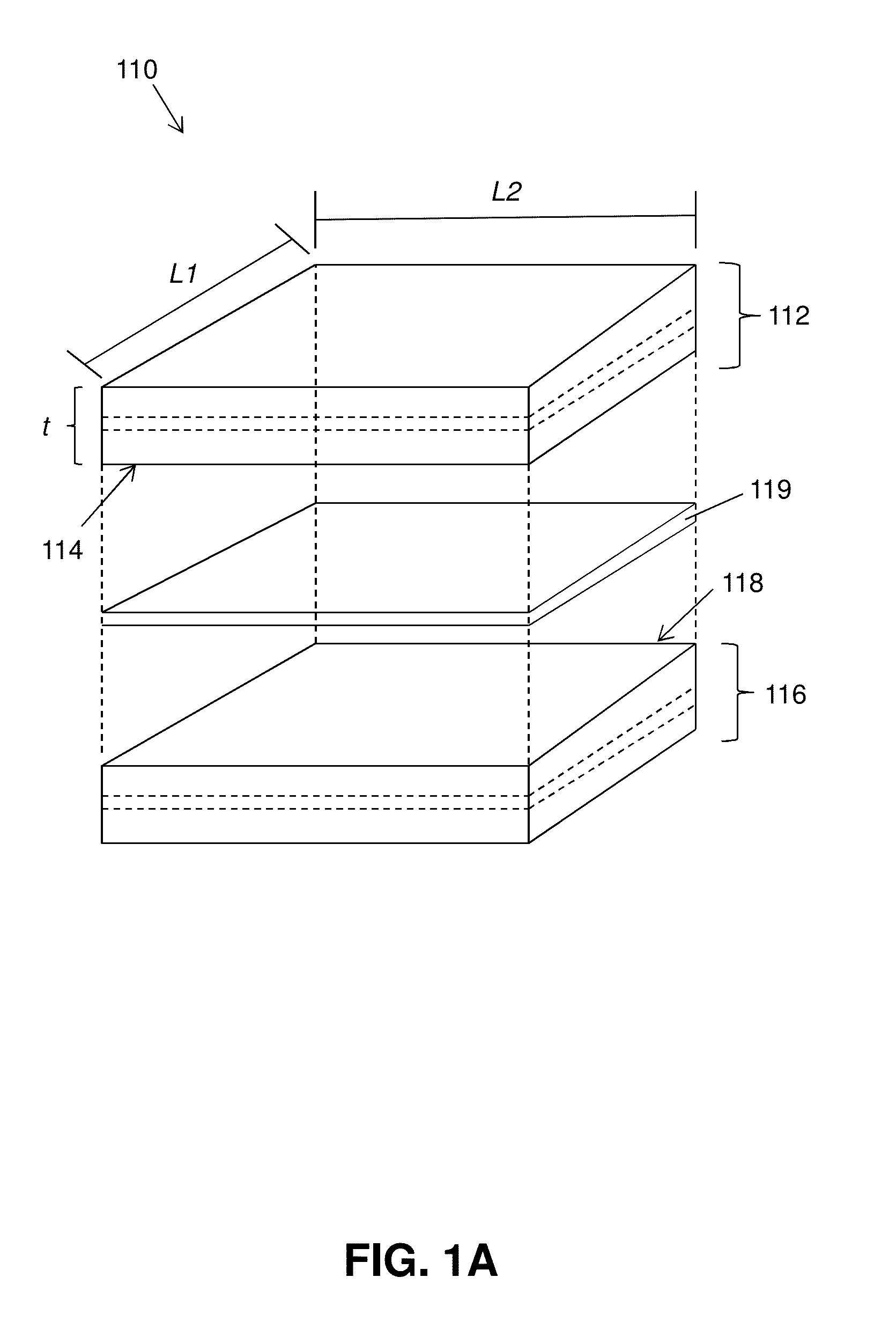
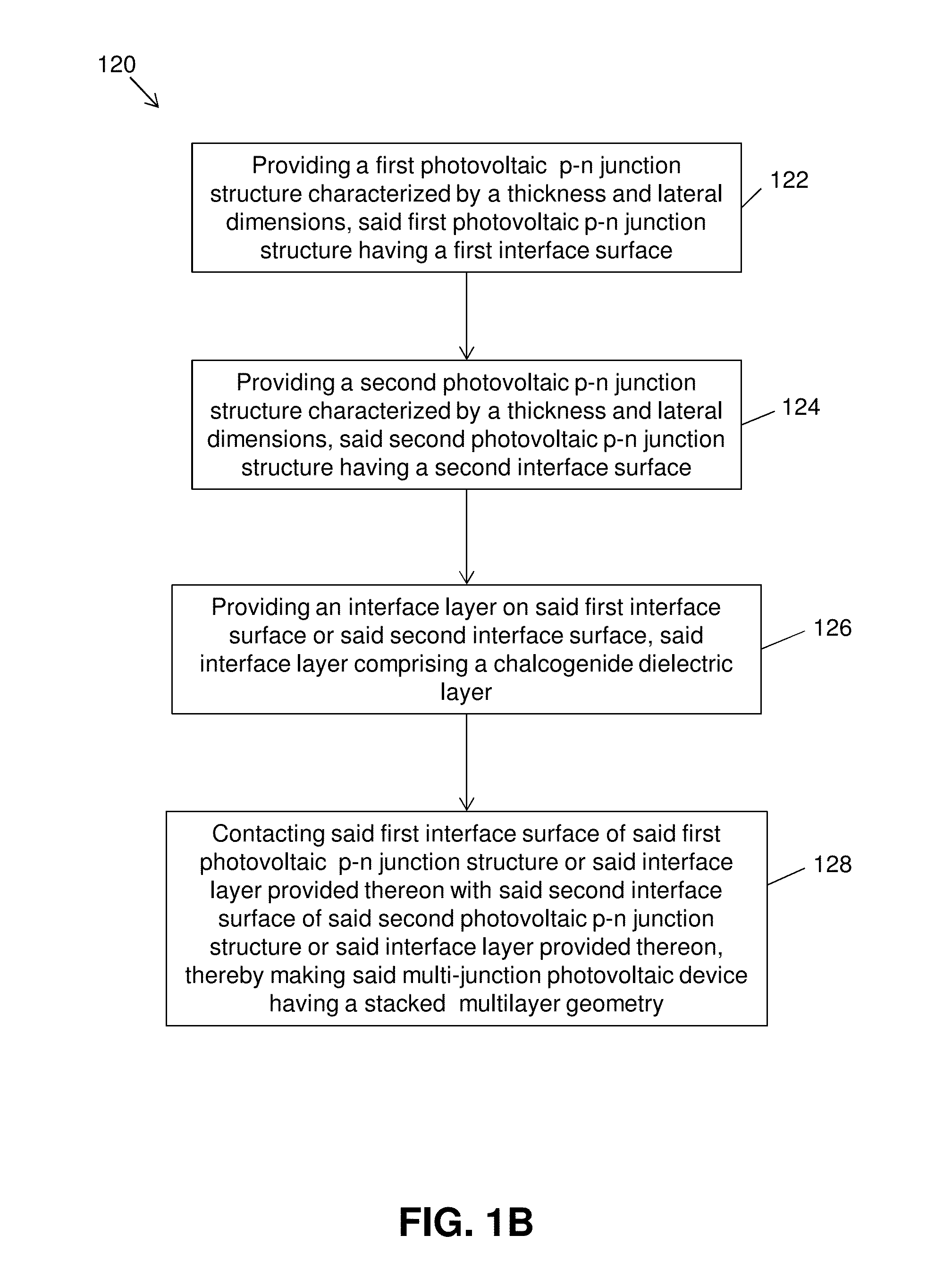
[0205]Multijunction (MJ) solar cells have the potential to operate across the entire solar spectrum, for ultrahigh efficiencies in light to electricity conversion. This example presents an MJ cell architecture that offers enhanced capabilities in photon recycling and photon extraction, compared to those of conventional devices. Ideally, each layer of a MJ cell should recycle and re-emit its own luminescence to achieve the maximum possible voltage. The present design involves materials with low refractive indices as interfaces between sub-cells in the MJ structure. Experiments demonstrate that thin-film GaAs devices printed on low-index substrates exhibit improved photon recycling, leading to increased open-circuit voltages (Voc), consistent with theoretical predictions. Additional systematic studies reveal important considerations in the thermal behavior of these structures under highly ...


PUM


Abstract

Multi-junction photovoltaic devices and methods for making multi-junction photovoltaic devices are disclosed. The multi-junction photovoltaic devices comprise a first photovoltaic p-n junction structure having a first interface surface, a second photovoltaic p-n junction structure having a second interface surface, and an optional interface layer provided between the first interface surface and the second interface surface, where the photovoltaic p-n junction structures and optional layers are provided in a stacked multilayer geometry. In an embodiment, the optional interface layer comprises a chalcogenide dielectric layer.

Description

CROSS-REFERENCE TO RELATED APPLICATIONS[0001]This application claims benefit to U.S. Provisional Patent Application No. 61 / 928,364 filed Jan. 16, 2014, which is incorporated by reference to the extent not inconsistent herewith.STATEMENT REGARDING FEDERALLY SPONSORED RESEARCH OR DEVELOPMENT[0002]Not applicable.BACKGROUND OF INVENTION[0003]Significant research activity has sought to realize the efficiency limits of known photovoltaic (PV) cells, and to expand upon materials and geometries for semiconductor p-n junctions in order to increase cell efficiency.[0004]Single junction (SJ) cells have a theoretical efficiency limit of ˜33.4% under one sun illumination, primarily due to the ineffective use of the entire solar spectrum. To optimize the efficiency of SJ cells, multiple, separated SJ cells can be implemented with spectral-splitting optical elements to utilize more of the solar spectrum, but complexity in manufacturing, alignment and light management hinders use of such systems in...

Claims


Application Information

Patent Timeline
IPC IPC(8): H01L31/0725H01L31/0216H01L31/0232H01L31/0735H01L31/18
CPCH01L31/0725H01L31/0735H01L31/02168H01L31/1844H01L31/02327H01L31/184Y02E10/544H01L31/03046H01L31/03048H01L31/0687H01L31/1892H01L31/043Y02P70/50
Inventor ROGERS, JOHN A.SHENG, XINGBOWER, CHRISTOPHER A.MEITL, MATTHEWBURROUGHS, SCOTT
Owner THE BOARD OF TRUSTEES OF THE UNIV OF ILLINOIS
Why Eureka
Try Eureka