Light emitting device and method of manufacturing light emitting device

Active Publication Date: 2015-07-23
NICHIA CORP
View PDF6 Cites 20 Cited by
  • Summary
  • Abstract
  • Description
  • Claims
  • Application Information

AI Technical Summary

Benefits of technology

[0013]In a light emitting device according to the embodiments of the present invention, the wavelength conversion layer having the uniform thickness is formed on the upper surface and the side surfaces serving as a light extracting surface of the semiconductor light emitting element, and the wavelength conversion layer is not excessively formed at the lower portion of the side surfaces, so that it is possible to reduce the unevenness in distribution light color. In addition, in a method of manufacturing the light emitting device according to the embodiments o

Problems solved by technology

Thus, if the LED chip is not correctly aligned with the stencil mask, it may result in occurrence of some regions where the wavelength conversion layer is not formed in the upper surface, and the wavelength conversion layer does not have a predetermined thickness on the side surface, so that uneven distribution of light color may occur.
According to the other method, at the time of dicing the wavelength conversion layer applied to the LED chips, if the position to be diced is not accurate, the wavelength conversion layer provided on the side surface does not have a predetermined thickness, so that a distribution light color becomes uneven.
In addition, according to the method disclosed in JP 2

Method used


Image

  • Light emitting device and method of manufacturing light emitting device
  • Light emitting device and method of manufacturing light emitting device
  • Light emitting device and method of manufacturing light emitting device

Examples


Example

First Embodiment

Configuration of Light Emitting Device

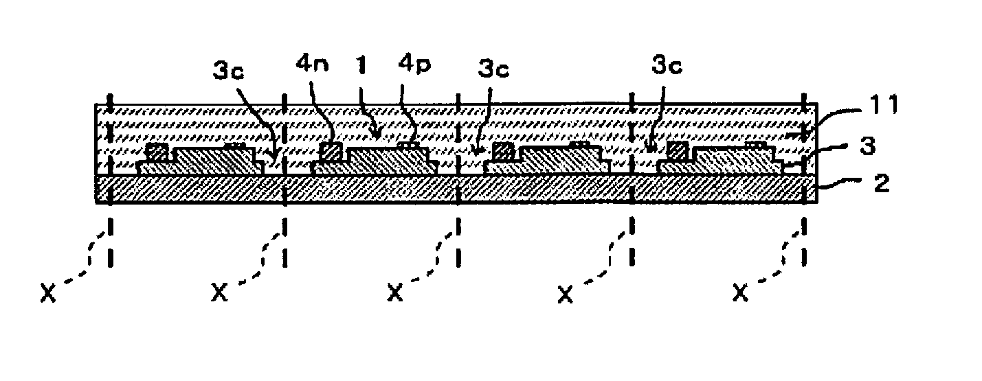
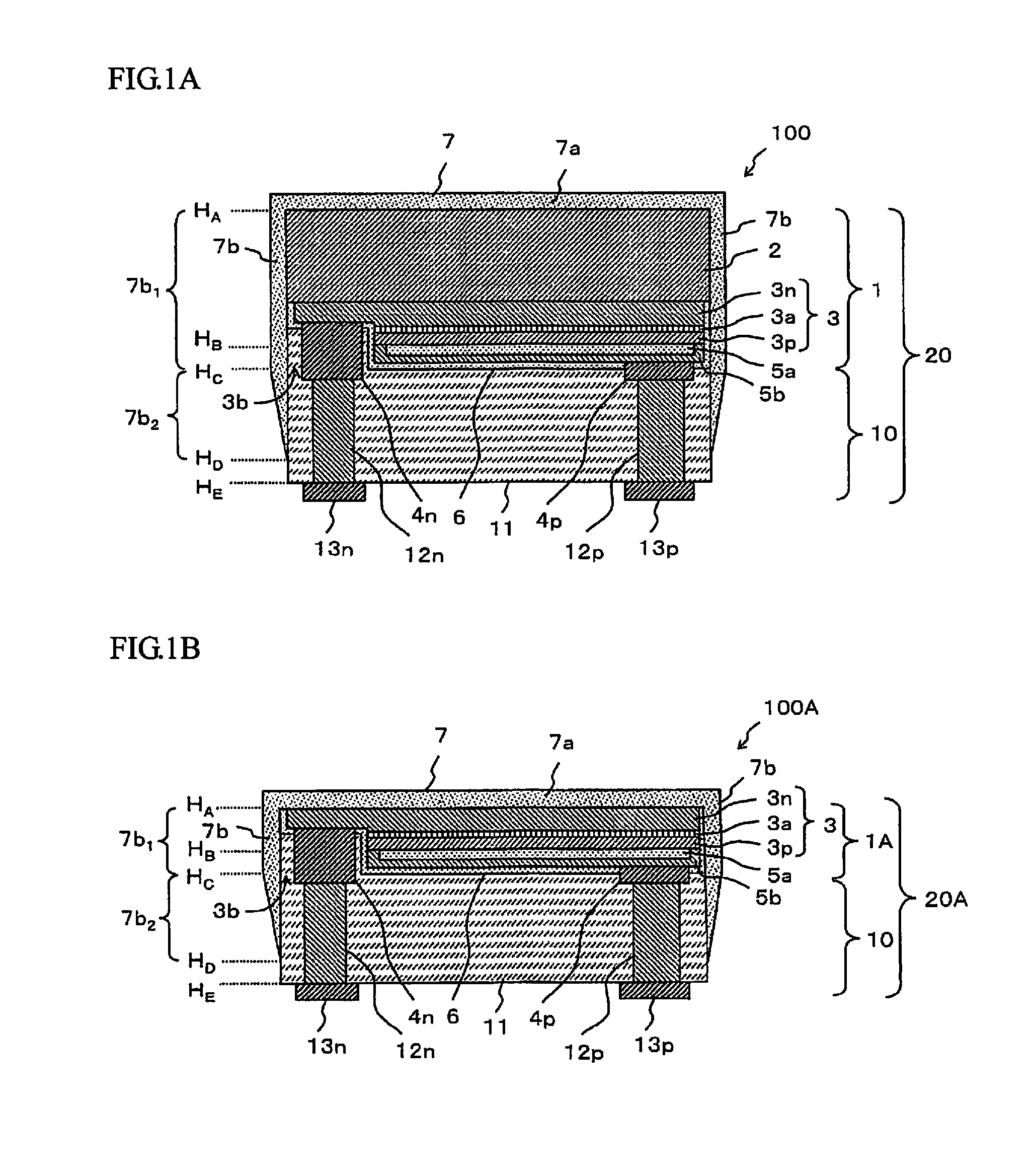
[0026]First, a configuration of a light emitting device according to a first embodiment of the present invention will be described with reference to FIG. 1A. As shown in FIG. 1A, a light emitting device 100 according to the present embodiment includes a supporting body 10, a semiconductor light emitting element 1 (hereinafter may be referred to as “light emitting element”) provided on the supporting body 10, and a phosphor layer (wavelength conversion layer) 7 which covers an upper surface and side surfaces of the light emitting element 1, and upper side-surface portions of the supporting body 10. In the light emitting device 100, light (such as blue light) emitted from the light emitting element 1 is mixed with light (such as yellow light) provided in such a manner that the phosphor layer 7 partially absorbs the light emitted from the light emitting element 1 and converts its wavelength, and the mixed light (such as white light)...

Example

Second Embodiment

Configuration of Light Emitting Device

[0172]Next, a light emitting device according to a second embodiment will be described with reference to FIG. 9. As shown in FIG. 9, in a light emitting device 100D in the second embodiment, a light reflecting resin layer 14 is formed on the side surfaces of the supporting body 10, and the phosphor layer 7 is formed so as to cover an outer side of the reflecting resin layer 14. In a case where the resin layer 11 of the supporting body 10 is made of a light transmissive material, the light can be reflected and returned to the light emitting element 1 after being leaked from the lower surface and the side surfaces of the light emitting element 1 and propagated in the resin layer 11, so that there is an improvement in light extracting efficiency from the upper surface serving as the light extracting surface of the light emitting element 1. The light transmissive resin material also contains an element which partially absorbs the li...

Example

Third Embodiment

Configuration of Light Emitting Device

[0185]Next, a light emitting device according to a third embodiment will be described with reference to FIG. 10A. As shown in FIG. 10A, a light emitting device 100E in the third embodiment differs from the light emitting device 100A shown in FIG. 1B in that a supporting body 10E is provided instead of the supporting body 10. The supporting body 10E is provided such that the resin layer 11 covers the side surfaces of the light emitting element 1A, in addition to the lower surface of the light emitting element 1A. In addition, the resin layer 11 is made of a favorably reflecting resin obtained by mixing a light reflective filler in a light transmissive resin.

[0186]In the light emitting device 100E in the present embodiment, since the side surfaces of the light emitting element 1A are covered with the reflecting resin layer 11, the light is not extracted from the side surfaces of the light emitting device 100E, and the light is only...


PUM


Abstract

Provided is a light emitting device having a phosphor layer on a surface of a semiconductor light emitting element and reducing unevenness in light distribution color, and a method of manufacturing the same. A light emitting device 100 includes a light emitting element 20 with a supporting body which is composed of a semiconductor light emitting element 1 and a supporting body 10, and a phosphor layer 7 which continuously covers an upper surface and side surfaces of the semiconductor light emitting element 1, and side surfaces of the supporting body 10. The phosphor layer 7 is configured such that at least a lower portion of the side surface of the supporting body 10 is thinner than the upper surface and the side surface of the semiconductor light emitting element 1. Such a configuration of the phosphor layer can be formed by applying a spray-coating of a slurry containing phosphor particles and a thermosetting resin in a solvent on the semiconductor light emitting element 1 side of the light emitting element 20 which has the supporting body.

Description

CROSS-REFERENCE TO RELATED APPLICATION[0001]This application claims priority to Japanese Patent Application No. 2013-253474, filed on Dec. 6, 2013. The entire disclosure of Japanese Patent Application No. 2013-253474 is hereby incorporated herein by reference.BACKGROUND OF THE INVENTION[0002]1. Field of the Invention[0003]The present disclosure relates to a light emitting device including a semiconductor light emitting element and a wavelength conversion layer, and to a method of manufacturing the same.[0004]2. Description of Related Art[0005]There has been a white diode configured to emit white light by combining an LED (light emitting diode) to emit blue light and a wavelength conversion layer (phosphor layer) which absorbs a portion of the blue light emitted from the LED and converts the light to light of a different wavelength such as yellow light, are used in combination so that white light can be produced by mixing the blue light and the yellow light.[0006]A method of manufact...

Claims


Application Information

Patent Timeline
IPC IPC(8): H01L33/50H01L33/38H01L27/15H01L33/56
CPCH01L33/507H01L33/508H01L33/56H01L2933/0041H01L27/153H01L2933/005H01L33/38H01L33/501H01L2224/16225H01L33/505H01L33/486H01L33/502H01L2933/0033
Inventor IKEGAMI, TAKESHIHAYASHI, TADAOTAMAKI, HIROTO
Owner NICHIA CORP
Why Eureka
Try Eureka