Reduced Generation of Second Harmonics of FETs

a transistor and second harmonic technology, applied in the field of field effect transistor structure, can solve the problems of increasing second-order harmonics, and achieve the effects of reducing second-order harmonic distortion, and increasing second-order harmonics

Active Publication Date: 2015-08-06
PSEMI CORP
View PDF4 Cites 6 Cited by
  • Summary
  • Abstract
  • Description
  • Claims
  • Application Information

AI Technical Summary

Benefits of technology

[0016]The invention encompasses a structure and method for reducing second-order harmonic distortion in FETs used in applications that are sensitive to such distortion, such as switching RF signals. Measurements of FET architectures used in such applications has shown that the capacitance between drain and body is not equal to the capacitance between source and body for various device layout geometries, and that such asymmetry in capacitance modulates applied RF signals and results in an increase in second-order harmonics. Embodiments of the present invention include circuits and related layout geometries and corresponding methods for balancing out such asymmetry, thus reducing second-order harmonic distortion.

Problems solved by technology

Measurements of FET architectures used in such applications has shown that the capacitance between drain and body is not equal to the capacitance between source and body for various device layout geometries, and that such asymmetry in capacitance modulates applied RF signals and results in an increase in second-order harmonics.

Method used


Image

  • Reduced Generation of Second Harmonics of FETs
  • Reduced Generation of Second Harmonics of FETs
  • Reduced Generation of Second Harmonics of FETs

Examples


first embodiment

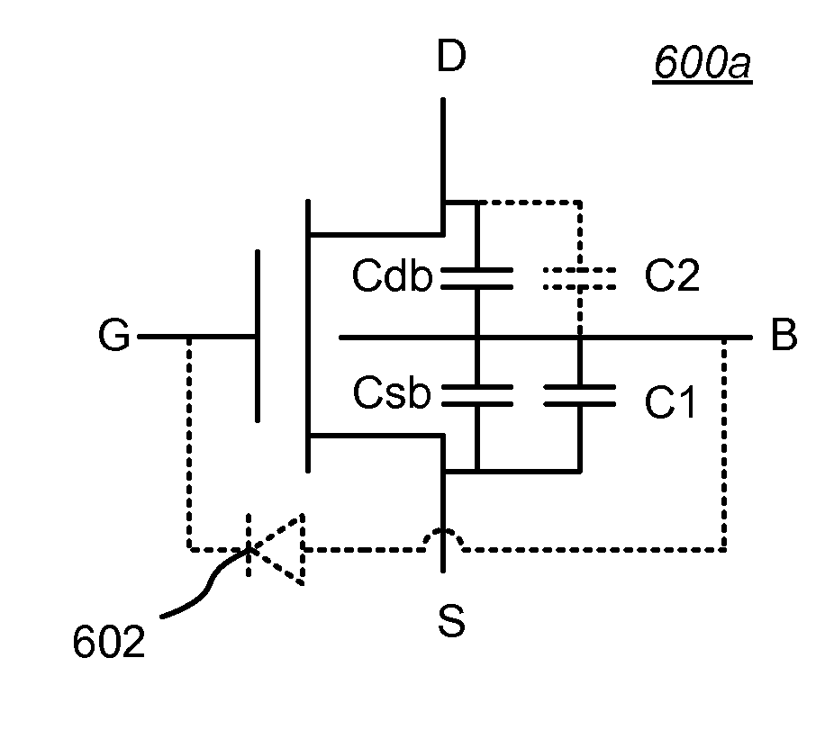
[0039]FIG. 6A is a FET 600a of the type shown in FIG. 1 and FIG. 5 modified in accordance with an aspect of the invention. In this embodiment, the layout-dependent drain-to-body capacitance Cdb is greater than the source-to-body capacitance Csb. This asymmetry is equalized by connecting at least a counter-balancing capacitance C1 between the source S and the body B. An optional body-to-gate diode 602 is shown as well. The capacitance value of C1 is sized to equalize the measured values of Cdb and Csb for a particular FET device layout geometry and size such that Csb+C1=Cdb.

second embodiment

[0040]FIG. 6B is a FET 600b of the type shown in FIG. 1 and FIG. 5 modified in accordance with an aspect of the invention. In this embodiment, the layout-dependent source-to-body capacitance Csb is greater than the drain-to-body capacitance Cdb. This asymmetry is equalized by connecting at least a counter-balancing capacitance C2 between the drain D and the body B. An optional body-to-gate diode 602 is shown as well. The capacitance value of C2 is sized to equalize the measured values of Csb and Cdb for a particular FET device layout geometry and size such that Cdb+C2=Csb.

[0041]In both FIG. 6A and FIG. 6B, the added offsetting capacitance may be implemented as a distinct capacitor structure, as described more fully below. However, the added offsetting capacitance may also be implemented by re-arranging the geometry, size, and / or device materials of a FET so as to equalize the inherent parasitic capacitances of the device (i.e., the offsetting capacitance is implemented as a “purpose...

third embodiment

[0043]FIG. 7 is a FET 700 in accordance with an aspect of the invention, including an optional body-to-gate diode 702. In this embodiment, the asymmetry of the parasitic drain-to-body capacitance Cdb and source-to-body capacitance Csb of FIG. 5 (not shown in FIG. 7) is equalized by adding a bias voltage source Vds 704 to counter-balance the difference in charge accumulated by Cdb and Csb. The voltage provided by Vds will depend on the device layout geometry and size for a particular FET, but would typically be in the range of 10's to 100's of milli-volts.

[0044]The circuits shown in FIG. 6A and FIG. 6B are relatively easy to implement in a variety of ways. For example, FIG. 8A shows a top-down layout view of a FET 800a having an added drain-to-body and body-to-source capacitive layer in accordance with a first example embodiment of the present invention. The source region 802, the drain region 804, and the gate layer 806 are all formed in conventional fashion. In addition, a conducti...


PUM


Abstract

A structure and method for reducing second-order harmonic distortion in FET devices used in applications that are sensitive to such distortion, such as switching RF signals. The asymmetry of the drain-to-body capacitance Cdb and source-to-body capacitance Csb of a FET device are equalized by adding offsetting capacitance or a compensating voltage source.

Description

BACKGROUND[0001](1) Technical Field[0002]This invention generally relates to electronic circuits, and more specifically to field effect transistor structures.[0003](2) Background[0004]A field effect transistor (FET) employs a gate-modulated conductive channel between a source region and a drain region. Various types of FETs exist, including insulated gate FETs (IGFETs), of which the most common type are metal-oxide-semiconductor FETs (MOSFETs). MOSFETs having n-type or p-type channel conductivity are referred to as an “NMOSFET” or “PMOSFET”, respectively.[0005]FIG. 1 is a schematic diagram of a conventional prior art FET 100 with an optional body diode. Shown are the source S, drain D, and gate G. Also shown is body connection B to the body or substrate on which the FET is fabricated. As is well known, when a voltage is applied between the gate G and source S terminals of a FET, a generated electric field penetrates through the gate oxide to the transistor body B. As one example, fo...

Claims


Application Information

Patent Timeline
Patent Type & Authority Applications(United States)
IPC IPC(8): H03K17/16
CPCH03K17/162H01L27/0629H01L29/1083H01L2924/30105
Inventor GENC, ALPER
Owner PSEMI CORP
Why Eureka
Try Eureka