RFID tag and micro chip integration design

a technology of integrated microchips and RFID tags, which is applied in the direction of programmable/customizable/modifiable circuits, instruments, and conductive patterns, etc., can solve the problems of reducing the power of the reader, limiting the communication distance up to several meters, and the electric field detected by the antenna is much weaker than the electric field, so as to reduce the area of the micro rfid chip, reduce stress, and reduce the size of the micro r

Active Publication Date: 2015-08-20
APPLE INC
View PDF2 Cites 32 Cited by
  • Summary
  • Abstract
  • Description
  • Claims
  • Application Information

AI Technical Summary

Benefits of technology

[0009]In accordance with embodiments of the invention, the area of the micro RFID chip can be reduced by using lower technology modes for logic, for example, below 0.180 μm. Reduction of size of the micro RFID chip may also reduce stress. In a...

Problems solved by technology

The available power from the reader reduces rapidly with distance and is generally regulated resulting in limited communication distances up to several meters.
As a result the electric field detected by the antenna can be much weaker than the electric field that would be ...

Method used


Image

  • RFID tag and micro chip integration design
  • RFID tag and micro chip integration design
  • RFID tag and micro chip integration design

Examples


Embodiment Construction

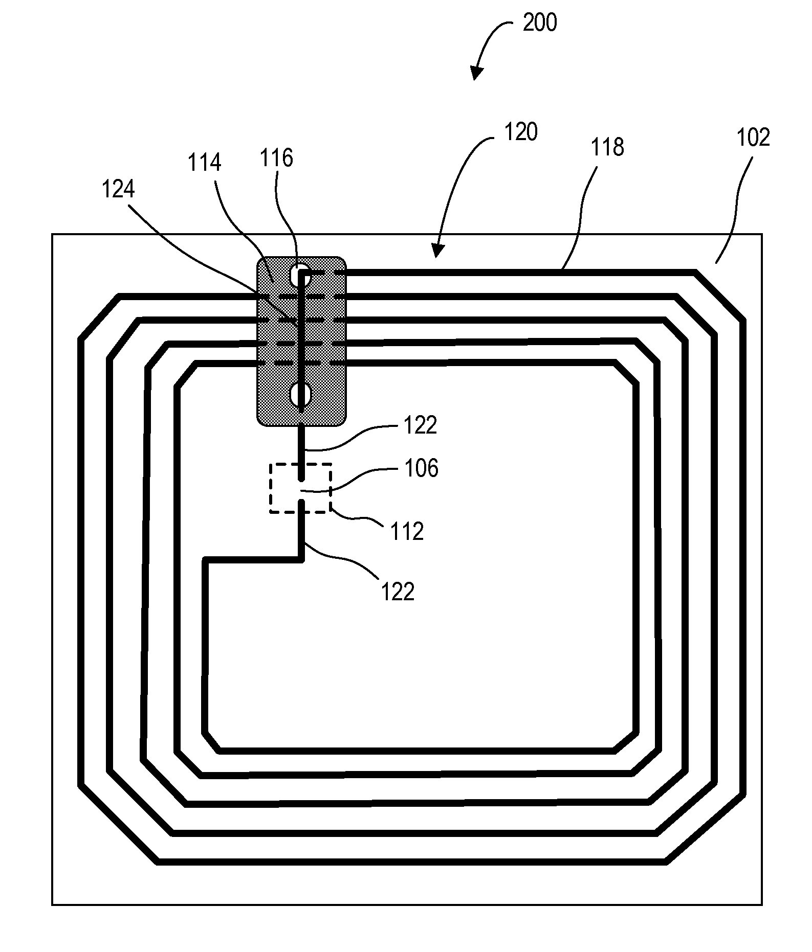
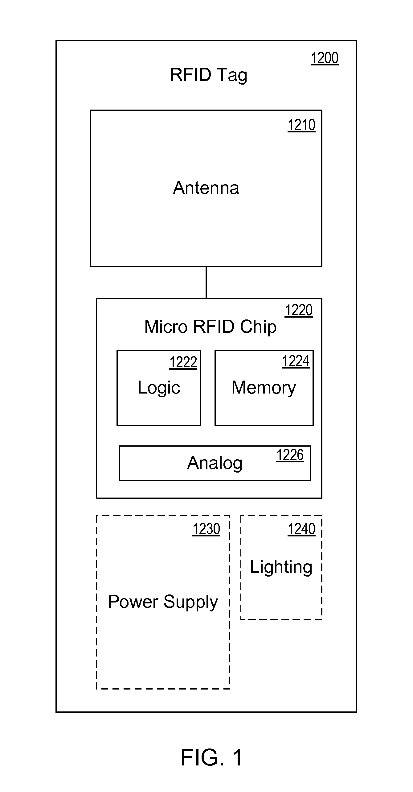
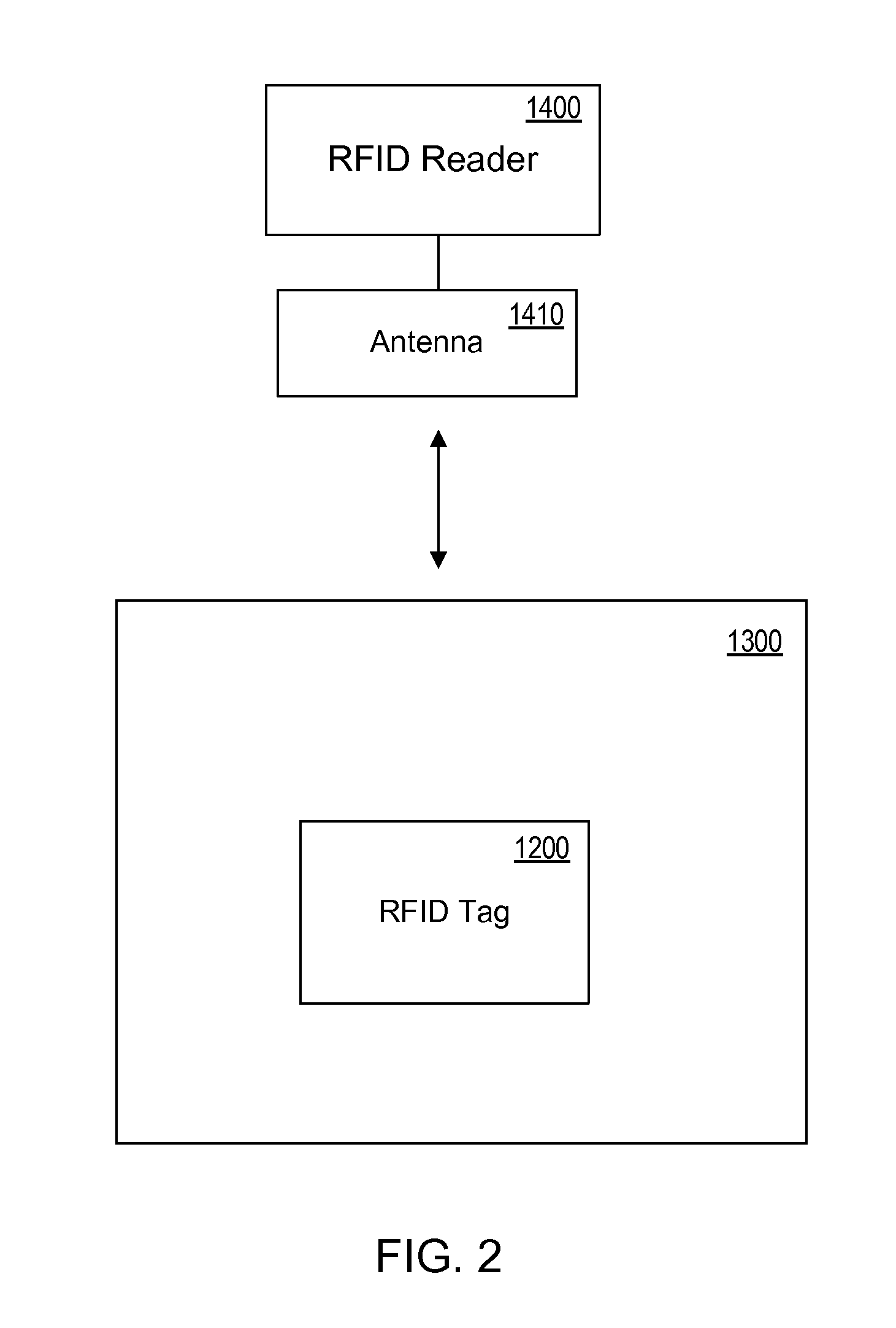
[0027]Embodiments of the present invention describe designs and systems for integrating micro chips. In an embodiment a micro chip is bonded to opposite sides of a line break in a conductive pattern. In some embodiments, the conductive pattern is formed on a substrate, followed by cutting (for example, by laser ablation), which is followed by electrostatic transfer and bonding of the micro chip to the conductive pattern. While some embodiments of the present invention are described with specific regard to micro chips for RFID applications, it is to be appreciated that embodiments of the invention are not so limited and that certain embodiments may also be applicable to other integration designs such as integrated passive device (IPD) chips, MEMS, etc.

[0028]In various embodiments, description is made with reference to figures. However, certain embodiments may be practiced without one or more of these specific details, or in combination with other known methods and configurations. In ...


PUM

PropertyMeasurementUnit
Lengthaaaaaaaaaa
Lengthaaaaaaaaaa
Widthaaaaaaaaaa

Abstract

An integrated micro chip, method of integrating a micro chip, and micro chip integration system are described. In an embodiment, a micro chip such as a micro RFID chip or integrated passive device (IPD) is electrostatically transferred and bonded to a conductive pattern including a line break. In an embodiment, the line break is formed by a suitable cutting technique such as laser laser ablation, ion beam etching, or photolithography with chemical etching to accommodate the micro chip.

Description

BACKGROUND[0001]1. Field[0002]The present invention relates to integrated micro chip applications. More particularly embodiments of the present invention relate to an RFID tag with an integrated micro chip.[0003]2. Background Information[0004]Radio frequency identification (RFID) is a manner of identifying objects with a wireless communication protocol. The technology can be used to identify, track, sort or detect a wide variety of objects. An RFID system generally includes an RFID tag and a reader. Passive RFID tags include an integrated circuit or chip and an antenna, and are powered by an electromagnetic field provided by the reader. The available power from the reader reduces rapidly with distance and is generally regulated resulting in limited communication distances up to several meters. Passive RFID tags can be operated over the entire frequency range available to RFID systems including low frequency (LF; <300 kHz; 125 kHz primary frequency), high frequency (HF; 3 MHz-30 M...

Claims


Application Information

Patent Timeline
IPC IPC(8): G06K19/077H05K3/20H05K3/14H05K3/34H05K3/12
CPCG06K19/07783H05K1/0293H05K1/165H05K2201/10098H05K2203/107H05K2203/175Y10T29/49144Y10T29/53174
Inventor PAVATE, VIKRAMBIBL, ANDREAS
Owner APPLE INC
Why Eureka
Try Eureka