Optical imaging lens and electronic device comprising the same
a technology of optical imaging and electronic devices, applied in the field of optical imaging lens sets and electronic devices, can solve the problems that the size of the optical imaging lens sets is too large to meet the specification requirements of consumer electronics products, and the conventional optical imaging lens sets of four lens elements can hardly meet these requirements, and achieve the effects of low production cost, high image quality, and high resolution
- Summary
- Abstract
- Description
- Claims
- Application Information
AI Technical Summary
Benefits of technology
Problems solved by technology
Method used
Image

Examples
first example
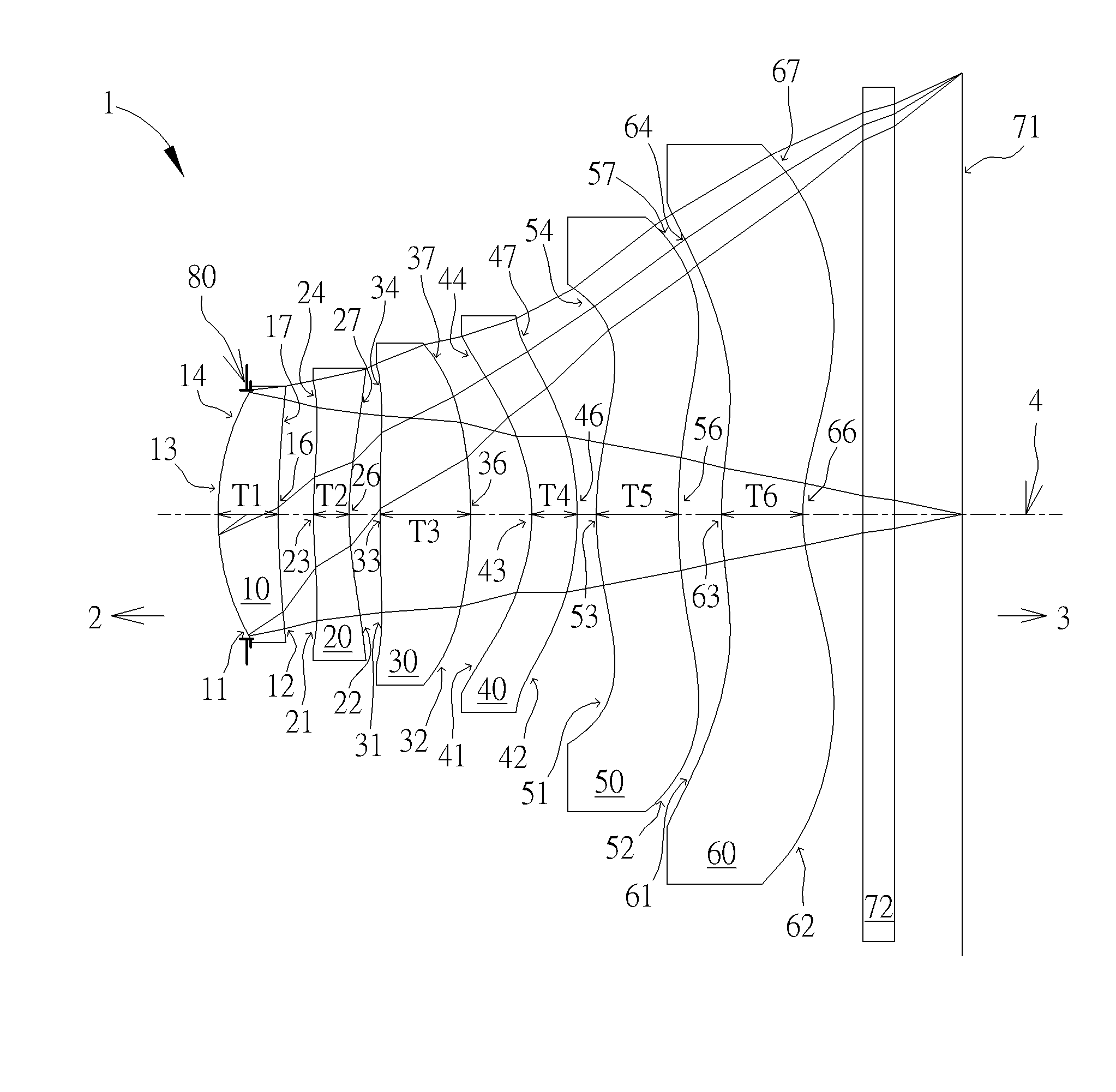
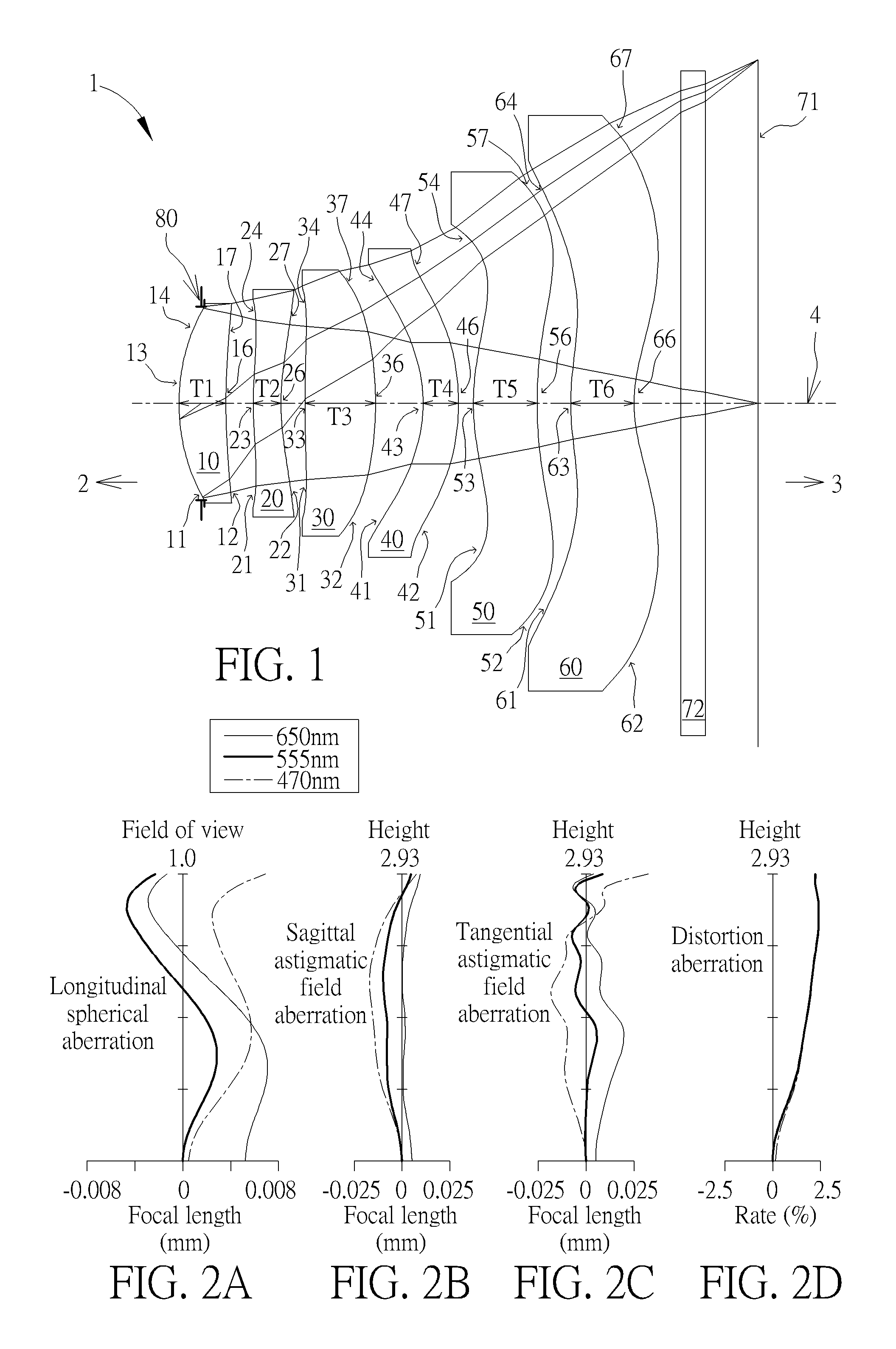
[0107]Please refer to FIG. 1 which illustrates the first example of the optical imaging lens set 1 of the present invention. Please refer to FIG. 2A for the longitudinal spherical aberration on the image plane 71 of the first example; please refer to FIG. 2B for the astigmatic field aberration on the sagittal direction; please refer to FIG. 2C for the astigmatic field aberration on the tangential direction, and please refer to FIG. 2D for the distortion aberration. The Y axis of the spherical aberration in each example is “field of view” for 1.0. The Y axis of the astigmatic field and the distortion in each example stand for “image height”. The image height is 2.93 mm.
[0108]The optical imaging lens set 1 of the first example has six lens elements 10 to 60 are made of a plastic material and have refractive power. The optical imaging lens set 1 also has an aperture stop 80, a filter 72, and an image plane 71. The aperture stop 80 is provided between the object side 2 and the first len...
second example
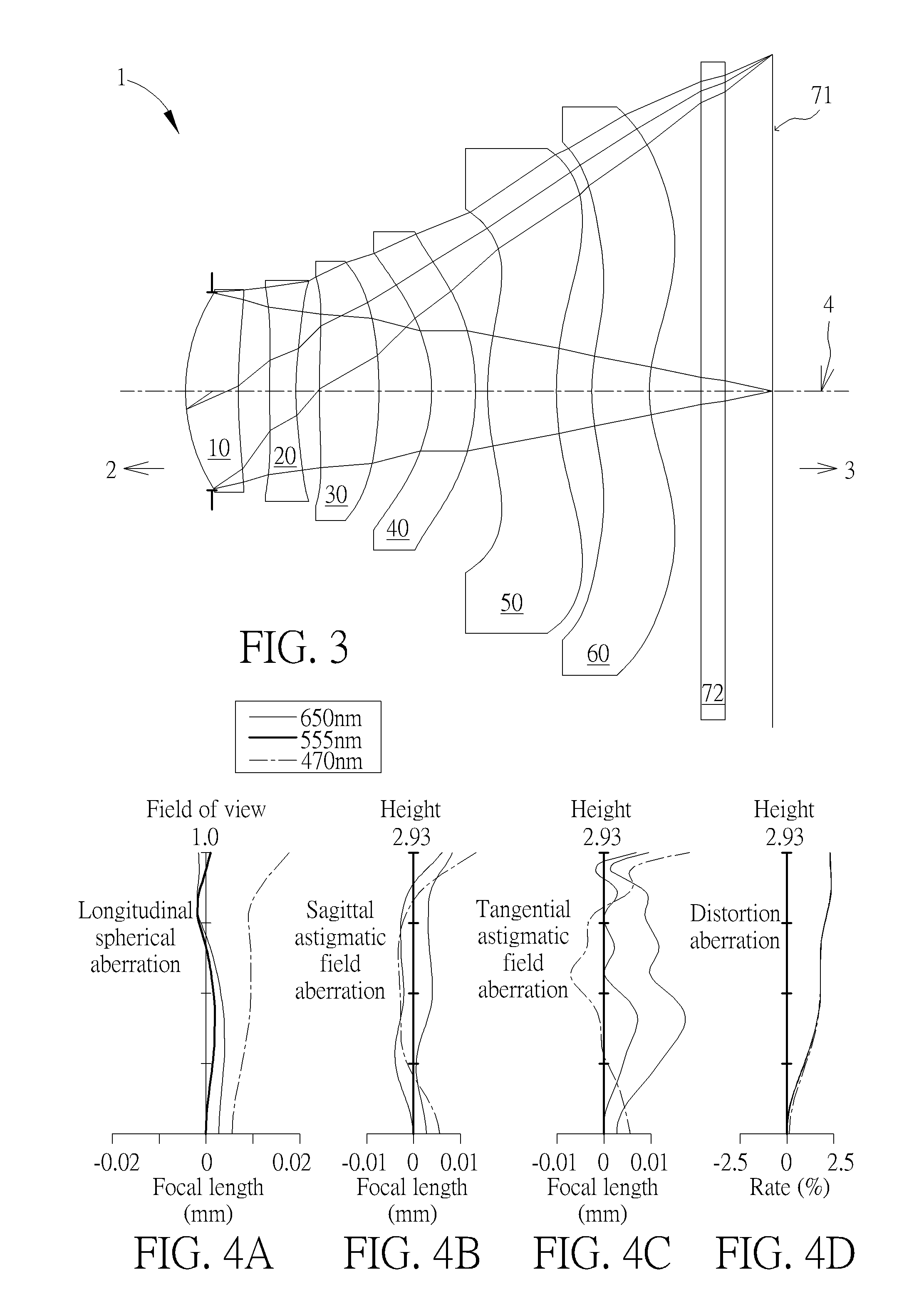
[0122]Please refer to FIG. 3 which illustrates the second example of the optical imaging lens set 1 of the present invention. It is noted that from the second example to the following examples, in order to simplify the figures, only the components different from what the first example has and the basic lens elements will be labeled in figures. Others components that are the same as what the first example has, such as the object-side surface, the image-side surface, the part in a vicinity of the optical axis and the part in a vicinity of its circular periphery will be omitted in the following example. Please refer to FIG. 4A for the longitudinal spherical aberration on the image plane 71 of the second example; please refer to FIG. 4B for the astigmatic aberration on the sagittal direction; please refer to FIG. 4C for the astigmatic aberration on the tangential direction, and please refer to FIG. 4D for the distortion aberration. The components in the second example are similar to tho...
third example
[0123]Please refer to FIG. 5 which illustrates the third example of the optical imaging lens set 1 of the present invention. Please refer to FIG. 6A for the longitudinal spherical aberration on the image plane 71 of the third example; please refer to FIG. 6B for the astigmatic aberration on the sagittal direction; please refer to FIG. 6C for the astigmatic aberration on the tangential direction, and please refer to FIG. 6D for the distortion aberration. The components in the third example are similar to those in the first example, but the optical data such as the curvature radius, the refractive power, the lens thickness, the lens focal length, the aspheric surface or the back focal length in this example are different from the optical data in the first example, and in this example, the third object-side surface 31 of the third lens element 30 has a convex part 33A in the vicinity of the optical axis and a convex part 34A in a vicinity of its circular periphery. The optical data of ...
PUM
 Abstract
Description
Claims
Application Information
 - R&D
- Intellectual Property
- Life Sciences
- Materials
- Tech Scout
- Unparalleled Data Quality
- Higher Quality Content
- 60% Fewer Hallucinations
Browse by: Latest US Patents, China's latest patents, Technical Efficacy Thesaurus, Application Domain, Technology Topic, Popular Technical Reports.
© 2025 PatSnap. All rights reserved.Legal|Privacy policy|Modern Slavery Act Transparency Statement|Sitemap|About US| Contact US: help@patsnap.com