Substrate cooling member, substrate processing device, and substrate processing method

a cooling member and substrate technology, applied in the direction of heat exchange apparatus, electric discharge tubes, lighting and heating apparatus, etc., can solve the problems of substrate deformation, complex structure, increased costs etc., to simplify the structure of the processing chamber, and reduce the cost of substrate processing apparatus

Inactive Publication Date: 2015-09-10
TOKYO ELECTRON LTD
View PDF0 Cites 6 Cited by
  • Summary
  • Abstract
  • Description
  • Claims
  • Application Information

AI Technical Summary

Benefits of technology

[0044]In the present disclosure, the gas is injected toward a substrate from the substrate cooling member, and a swirling flow is generated in the injected gas so that the substrate is efficiently cooled. This makes a conventional water cooling system needless which enables simplification of the structure of the processing chamber for cooling the substrate so that the processing chamber may be miniaturized. Further, miniaturization and cost reduction of the substrate processing apparatus become possible. In addition, in the case of the substrate processing apparatus which is provided with the processing chamber, of which the atmosphere is adjusted between a vacuum atmosphere and an atmospheric pressure atmosphere, the purge gas introduced into the processing chamber when the processing chamber is switched from the vacuum atmosphere to the atmospheric pressure atmosphere may be used for cooling the substrate. This makes the brake filter, which has been conventionally required for introducing a purge gas into a processing chamber, needless and thus, enables cost reduction of the substrate processing apparatus. In the present disclosure, a plurality of gas injection nozzles are provided in a region facing a central portion of the substrate so as to inject the gas to the substrate. This assists the cooling of the central portion of the substrate which is hardly cooled as compared to the peripheral portion of the substrate. Thus, it is possible to cool the substrate while suppressing deformation of the substrate without degrading throughput.

Problems solved by technology

In the substrate processing apparatus that requires a cooling system including the cooling table as described above, there are problems in that the structure is complicated and the volume of the intermediate conveyance chamber increases to enlarge the apparatus.
There is also a problem in that, due to the necessity of the cooling system, the costs of the substrate processing apparatus increase.
Thus, when the substrate is placed on the cooling table in the arc shape and held in that state, the peripheral portion, which is easily cooled, is in contact with the cooling table to be further cooled, but the central portion is in a floating state from the cooling table not to be cooled, so that a temperature distribution generated on the substrate increases, which may cause deformation on the substrate.
The deformation of the substrate may generate scratch on the rear surface of the substrate and damage a pattern (element) formed on the front surface of the substrate.

Method used


Image

  • Substrate cooling member, substrate processing device, and substrate processing method
  • Substrate cooling member, substrate processing device, and substrate processing method
  • Substrate cooling member, substrate processing device, and substrate processing method

Examples


Embodiment Construction

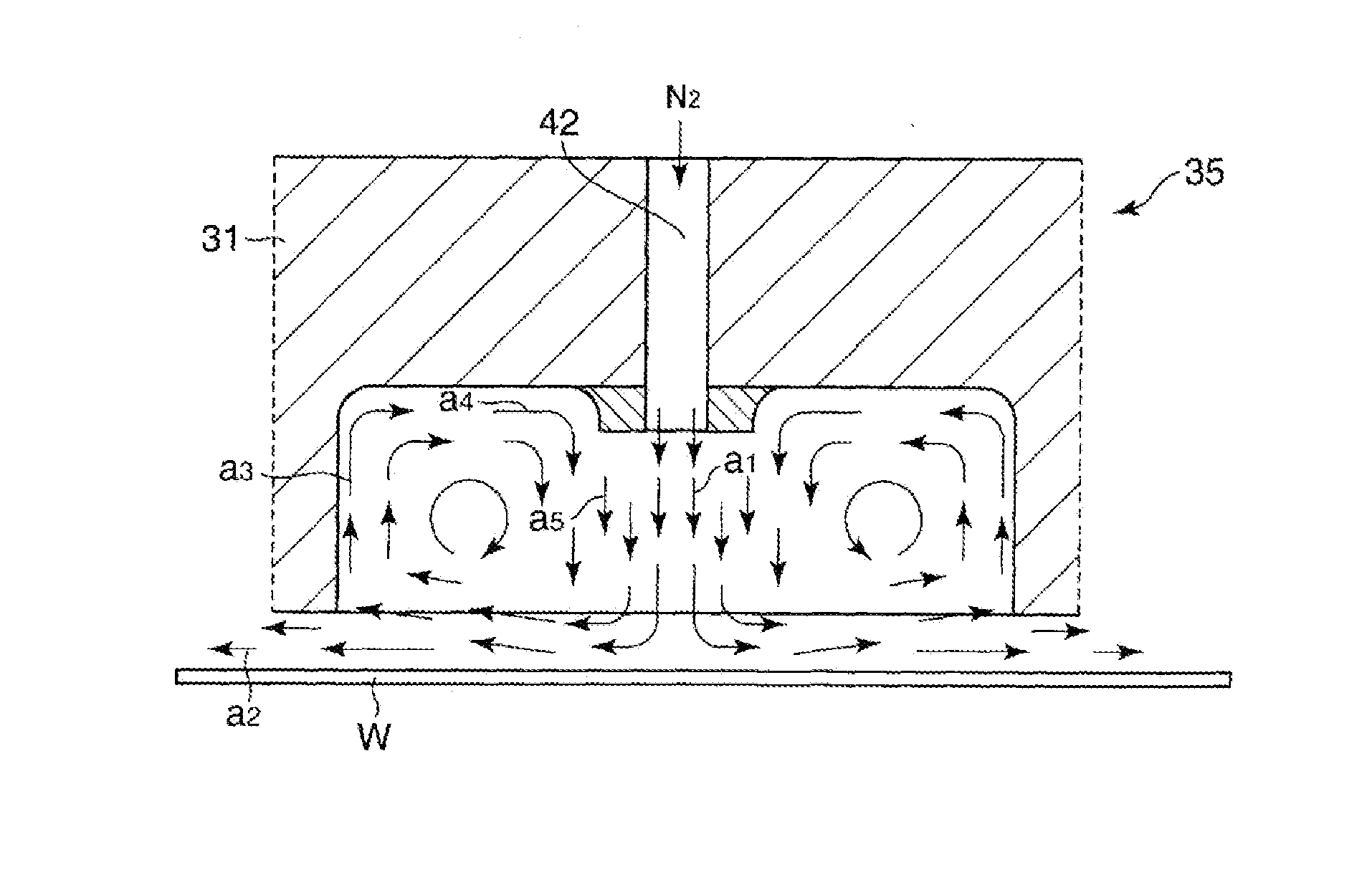
[0068]Hereinafter, exemplary embodiments of the present disclosure will be described in detail with reference to the accompanying descriptions. Here, as a substrate processing apparatus according to the present disclosure, a plasma processing apparatus that performs a plasma processing on a semiconductor wafer (hereinafter, referred to as a “wafer”) will be discussed.

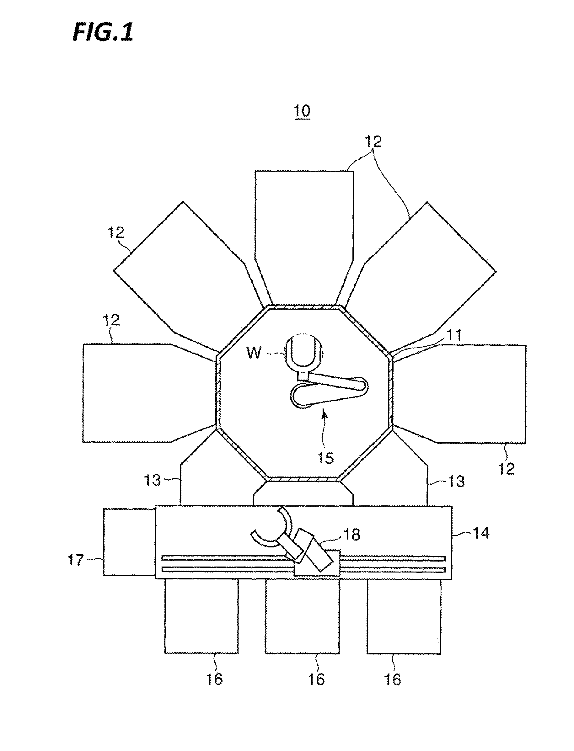
[0069]FIG. 1 is a plan view illustrating a schematic configuration of a plasma processing apparatus 10 according to an exemplary embodiment of the present disclosure. The plasma processing apparatus 10 is provided with three load ports 16 provided to dispose FOUPs (not illustrated) which are carriers that accommodate a predetermined number of wafers W having a diameter of 450 mm.

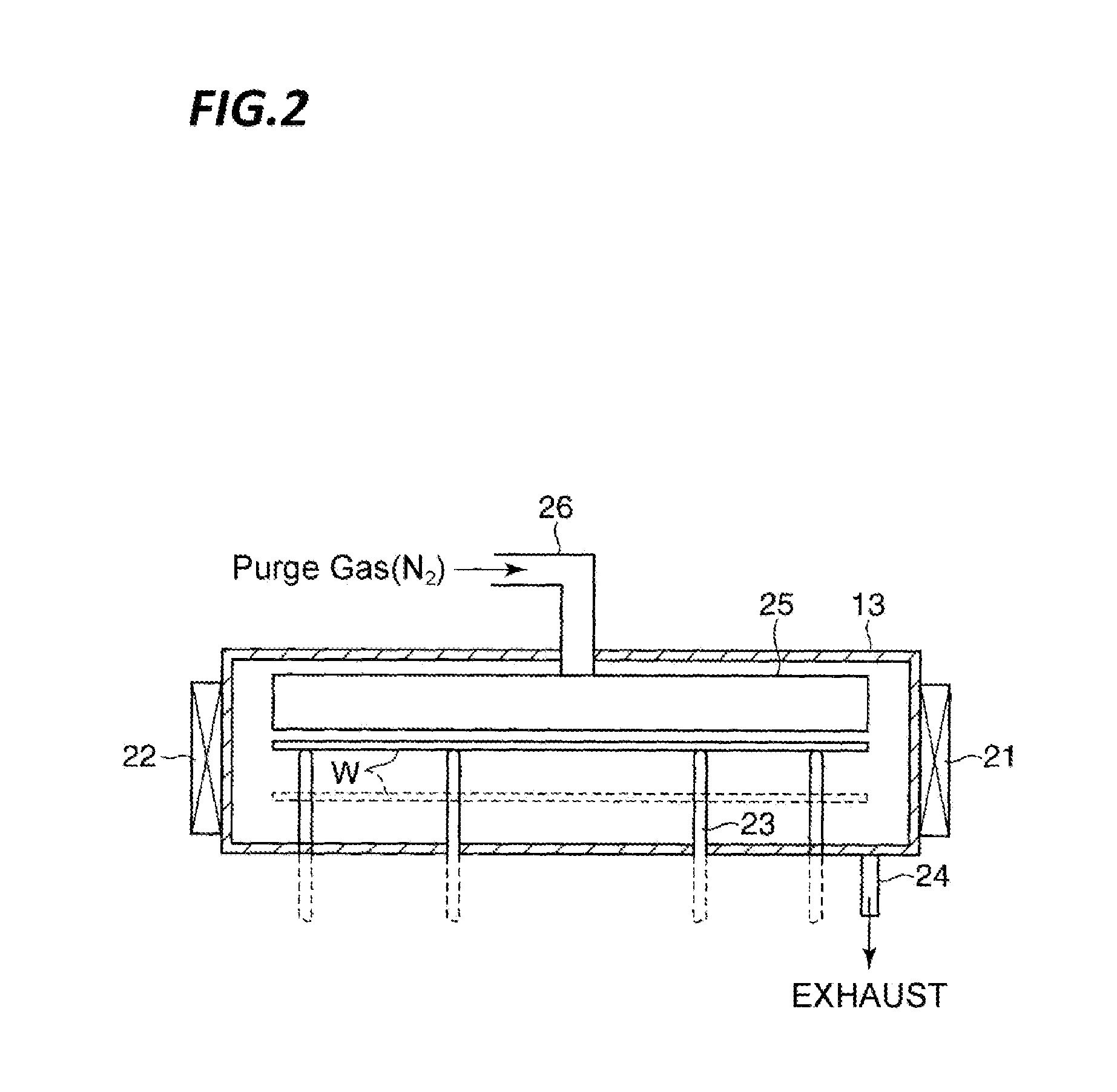
[0070]In the plasma processing apparatus 10, a loader module 14 is disposed adjacent to the load ports 16 so as to perform carry-in / carry-out of the wafers with respect to the FOUPS, and a positioning mechanism 17 is disposed adjacent to the loa...


PUM

PropertyMeasurementUnit
diameteraaaaaaaaaa
diameteraaaaaaaaaa
temperatureaaaaaaaaaa

Abstract

An objective of the present invention is to simplify a configuration of a processing chamber for cooling a substrate in a substrate processing device. In a plasma processing device (10) whereby a plasma process is carried out upon a wafer (W), the wafer (W) which is plasma processed is conveyed into a load-lock chamber (13), and gas is discharged from a gas discharge member (25) upon the surface of the wafer (W), cooling the wafer (W). The gas discharge member (25) comprises a structure wherein a plurality of gas discharge nozzles (35) are formed in one flat plate face of a flat plate member (31). The gas discharge nozzles (35) comprise cylindrical eddy generating chambers (41), and nozzle holes (42) which are opened in bottom walls (52) of the eddy generating chambers (41) and discharge the gas. The flat plate face of the wafer (W) and the flat plate face wherein the gas discharge nozzles (35) are formed in the flat plate member (31) are positioned in parallel at a prescribed gap. A purge gas is discharged from the nozzle holes (42) toward the wafer (W), and a flow of an eddy is made to arise in the discharged purge gas, thereby cooling the wafer (W), and simultaneously switching the interior of the load-lock chamber (13) from a vacuum environment to an atmospheric pressure environment.

Description

TECHNICAL FIELD[0001]The present disclosure relates to a substrate cooling member that cools a substrate such as, for example, a semiconductor wafer, a substrate processing apparatus including the substrate cooling member, and a substrate processing method using the substrate cooling member.BACKGROUND[0002]A substrate processing apparatus known in the related art includes a vacuum processing chamber that processes a substrate such as, for example, a semiconductor wafer, in a vacuum (decompressed) atmosphere and at a high temperature. In the substrate processing apparatus, it is required to cool a substrate processed in the vacuum processing chamber to a predetermined temperature and to carry the substrate out to the outside which is under an atmospheric pressure (e.g., a container that accommodates a plurality of substrates). Thus, the following process has been known.[0003]That is, the substrate processed in vacuum processing chamber is carried into an intermediate conveyance chamb...

Claims


Application Information

Patent Timeline
Patent Type & Authority Applications(United States)
IPC IPC(8): H01J37/32
CPCH01J37/32724H01J37/32733H01J37/32816H01J2237/334H01J37/32899H01J2237/002H01J37/32834H01L21/67109H01L21/67201H01J37/3244H01J37/32449H01J37/32522
Inventor KAWABE, ATSUSHIKOBAYASHI, SENSHO
Owner TOKYO ELECTRON LTD
Why Eureka
Try Eureka