Contact-Independent Electrical Conductance Measurement
a technology of electrical conductance and contact, which is applied in the direction of impedence measurement, resistance/reactance/impedence, instruments, etc., can solve the problems of limited operation, difficult to measure electrical conductance, and limited the ability to produce high-performance graphene transistors
- Summary
- Abstract
- Description
- Claims
- Application Information
AI Technical Summary
Benefits of technology
Problems solved by technology
Method used
Image

Examples
example i
Characterization of Element with Blocking Contacts
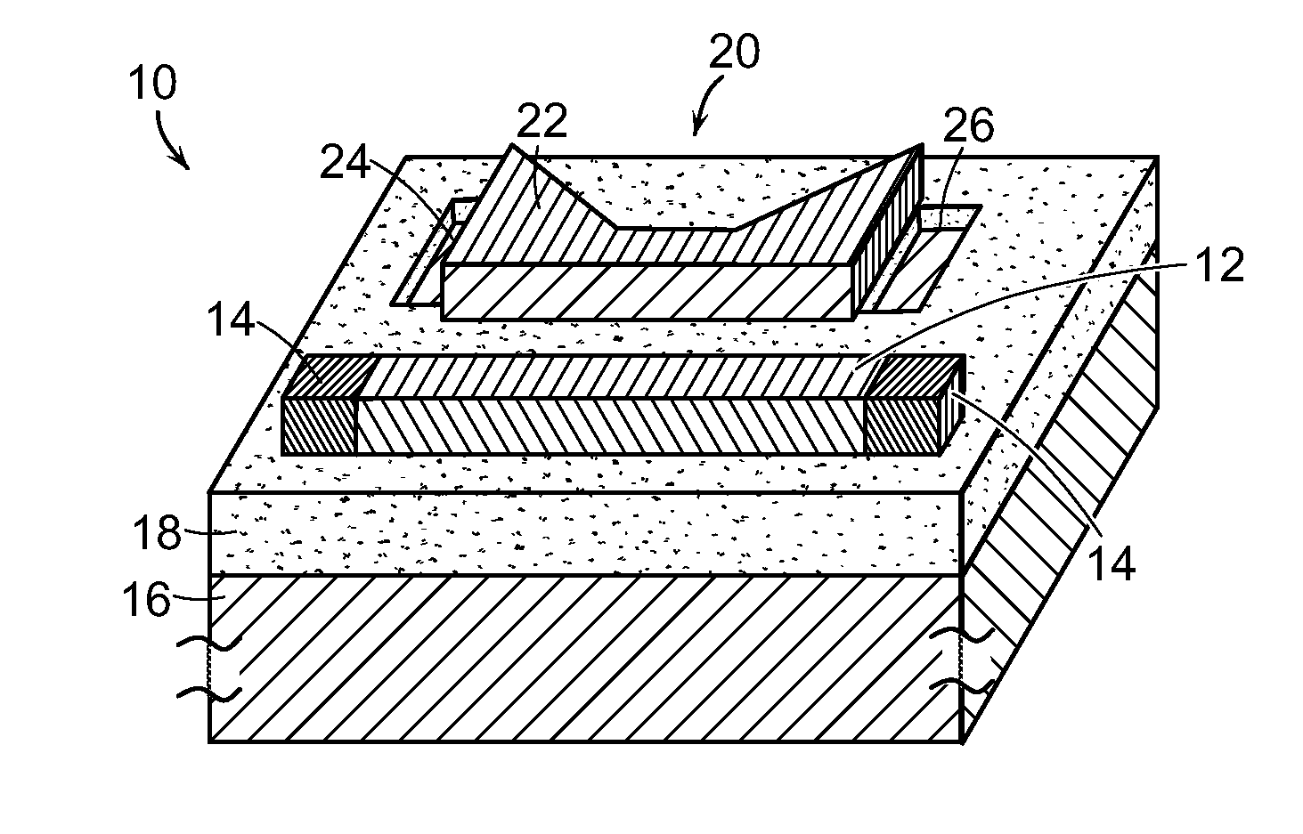
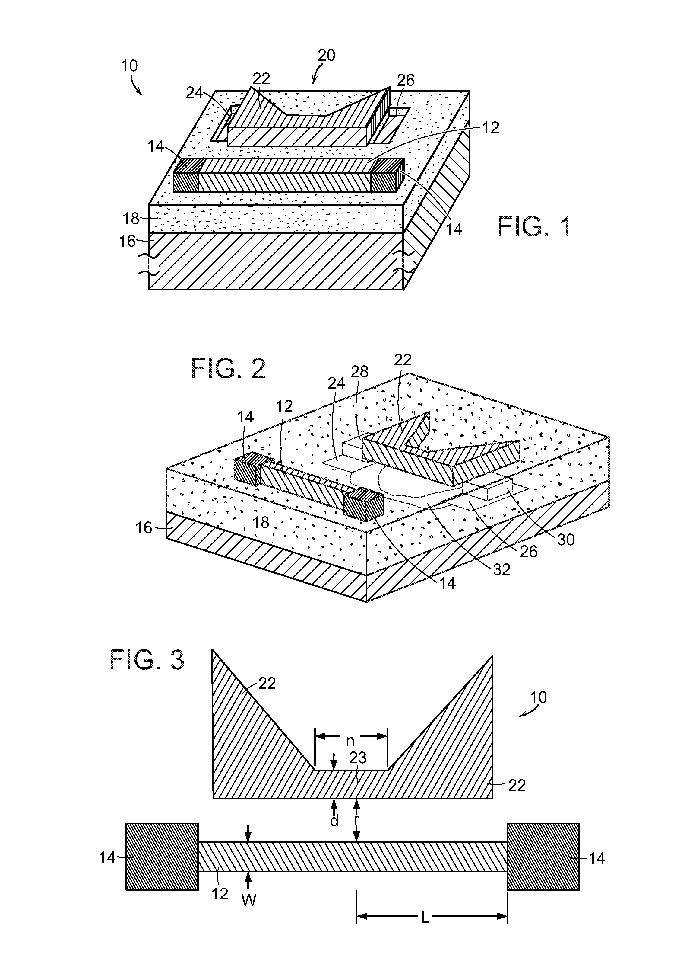
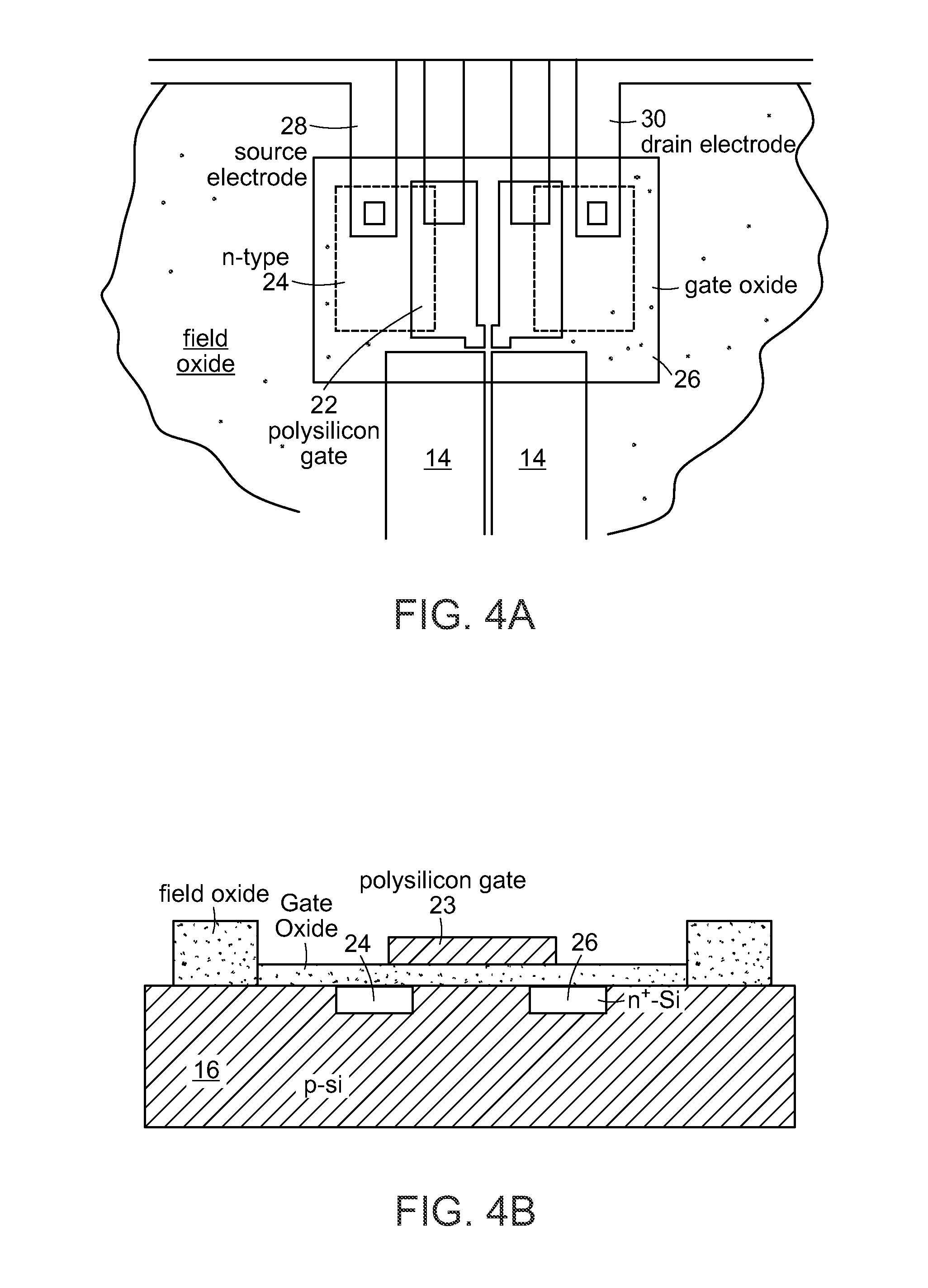
[0066]A conductance measurement system like that shown in FIG. 1 and FIG. 2 was fabricated, with an n-channel silicon MOSFET fabricated on a p-type silicon substrate, employing conventional CMOS techniques, in the manner described above. The gate of the MOSFET was tapered to a narrowed constriction region having a width of about 60 nm at its most narrow point.
[0067]An element for conductance measurement was fabricated a distance of about 100 nm from the MOSFET gate narrowing constriction. The element was fabricated as a thin film of amorphous germanium, patterned as a strip having a width of about 200 nm and a thickness of about 50 nm. The amorphous germanium strip was centered with center of the narrow constriction of the gate. Formation of the film of amorphous germanium was completed after evaporation of gold electrodes for contact to the germanium element.
[0068]The gold electrodes were disposed about 1 μm apart, giving a distance...
example ii
Characterization of MOSFET Conductance Sensor
[0071]The MOSFET of Example I was characterized to measure its sensitivity to nearby electrostatic fluctuations. Maintaining the MOSFET at a temperature of about 4 K, the gate voltage was swept from 3.6 V to 7.2 V and then back down to 3.6 V, and the conductance measured. FIG. 10A is a plot of the measured MOSFET conductance as a function of applied gate voltage. The oscillations in the conductance that are clear in the plot were nearly identical in both directions of voltage application. This is typical of a one-dimensional inversion layer where random fluctuations in the local potential at the Si / SiO2 interface cause oscillations in the conductance.
[0072]The gate voltage was then set to 8 V and the voltage between the source and drain, Vds, was set to 1 mV, so that the channel was in inversion, and the dc current in the MOSFET was measured as a function of time at a temperature of 11 K. FIG. 10B is a plot of the MOSFET conductance fluct...
example iii
Conductance Measurement
[0073]A conductance measurement of the amorphous germanium film of Example I was carried out with the MOSFET of Example I, with the geometric arrangement given. The biasing arrangement of FIG. 5 was employed. The voltage between the ends of the amorphous germanium film, Ve, as shown in FIG. 5, was stepped, so that charge flowed in the film, and simultaneously the conductance of the MOSFET was measured as a function of time. A positive voltage was maintained on the gate of the MOSFET, Vg>6V, to ensure that the channel was in inversion. A source-drain voltage, Vds, of 5 mV was set at one of the source or the drain contact, with current flow measured at the other of the source or the drain contact, using a Femto 400 kHz bandwidth amplifier 25 in FIG. 5. The source-drain voltage was ac, obtained with a transformer. The output of the current amplifier was monitored with a Stanford Research 830 lock-in amplifier.
[0074]The amplifiers, as well as voltage dividers and ...
PUM
 Abstract
Description
Claims
Application Information
 - R&D
- Intellectual Property
- Life Sciences
- Materials
- Tech Scout
- Unparalleled Data Quality
- Higher Quality Content
- 60% Fewer Hallucinations
Browse by: Latest US Patents, China's latest patents, Technical Efficacy Thesaurus, Application Domain, Technology Topic, Popular Technical Reports.
© 2025 PatSnap. All rights reserved.Legal|Privacy policy|Modern Slavery Act Transparency Statement|Sitemap|About US| Contact US: help@patsnap.com