Methods for reducing post layout circuit simulation results

Inactive Publication Date: 2015-09-24
ANALOG DESIGN AUTOMATION
View PDF7 Cites 21 Cited by
  • Summary
  • Abstract
  • Description
  • Claims
  • Application Information

AI Technical Summary

Benefits of technology

[0017]The present invention provides a method for creating and accessing post-layout circuit simulation results for examination. A method of the present invention reduces output file size—hence storage requirements—significantly, while improving circuit simulation speed. In addition, a method of the present invention reduces the number of nodes displayed, without lo

Problems solved by technology

However, as IC technology continues to advance, circuit simulation continues to require greater computing resources and time.
Consequently, circuit verification and debugging based on circuit simulation results have become the bottleneck in the design process of ICs.
Thus, a post-layout circuit simulation is typically significantly slower than the corresponding pre-layout circuit simulation.
The SPEF netlist is not SPICE-compatible, in that it cannot be read directly by most circuit simulators.
As the SPEF netlist is not suitable for analog circuit simulation, the SPEF netlist is not further considered here.
However, the back-annotation approach may be too error-prone for many applications, as back-annotation does not handle cross-talk capacitance or device back-annotation efficiently and correctly, especially for custom-designed circuits that have high simulation accuracy requirements.
Post-layout simulations can take up to hours, days or even weeks to complete.
These methods all suffer some accuracy loss, as the reduction ratio is always traded-off with error minimization.
However, in a method where the reduction technique is applied within the circuit simulator, the errors are more difficult to quantify, as how the reduction algorithm affect the results cannot not be readily ascertained.
Such forms of identification are very tedious to specify, especially when one needs to use node or circuit element names to map the post-layout nodes

Method used


Image

  • Methods for reducing post layout circuit simulation results
  • Methods for reducing post layout circuit simulation results
  • Methods for reducing post layout circuit simulation results

Examples


Embodiment Construction

[0048]Reference is now made in detail to one or more embodiments of the present invention. While the present invention is described in conjunction with these embodiments, such embodiments are not intended to be limiting the present invention. On the contrary, the present invention is intended to cover alternatives, variations, modifications and equivalents within the scope of the present invention, as defined in the accompanying claims.

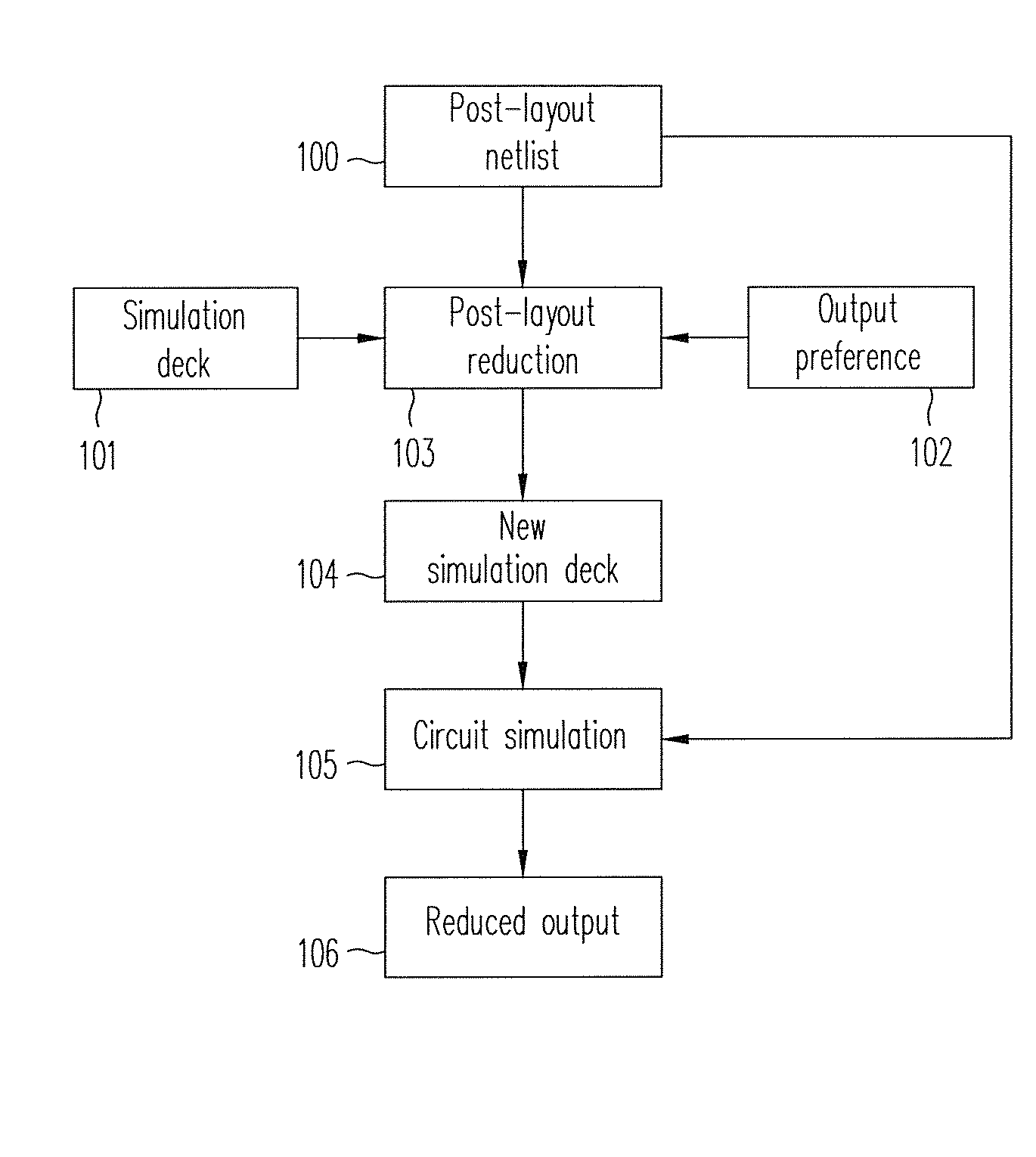
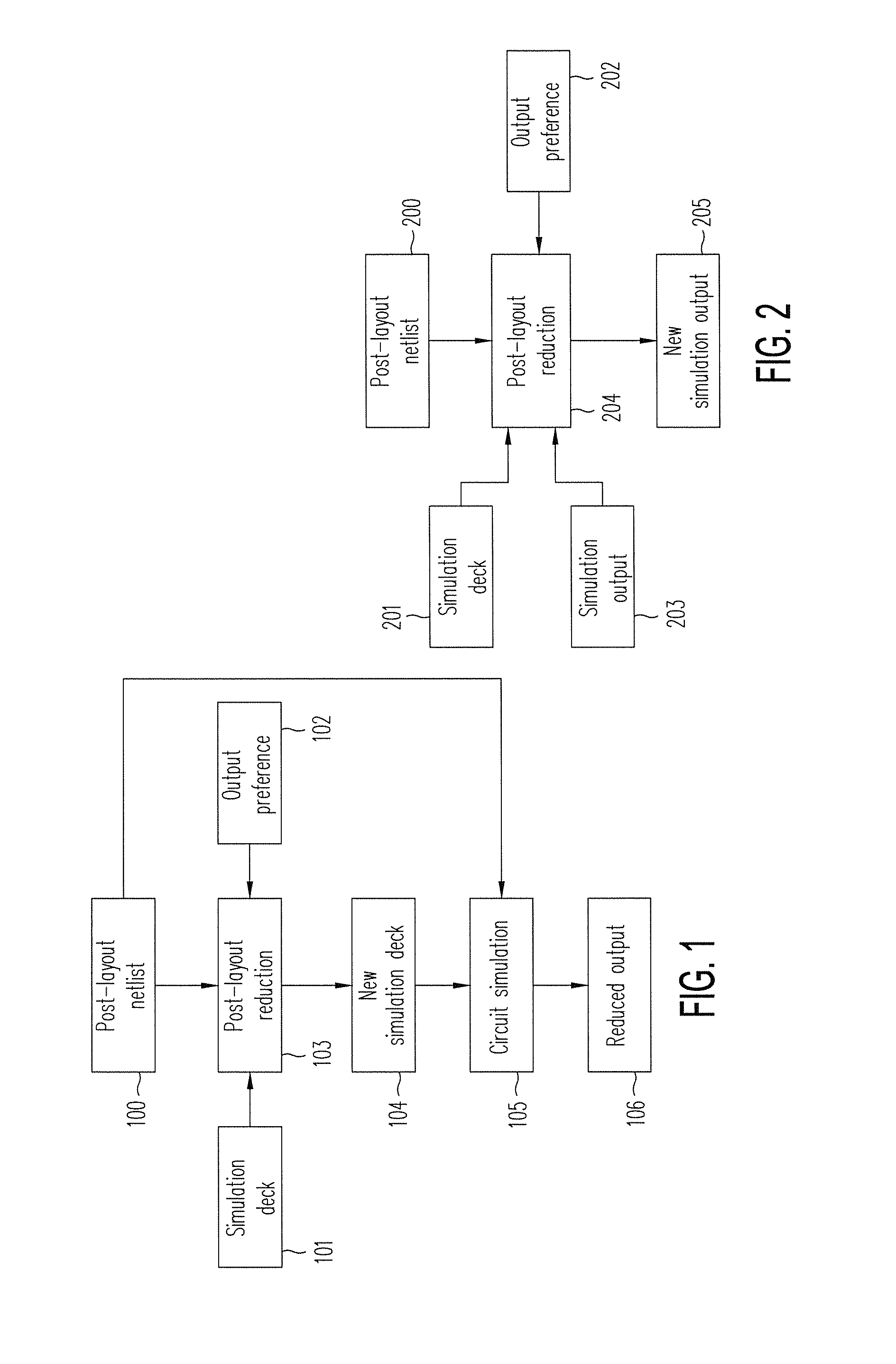
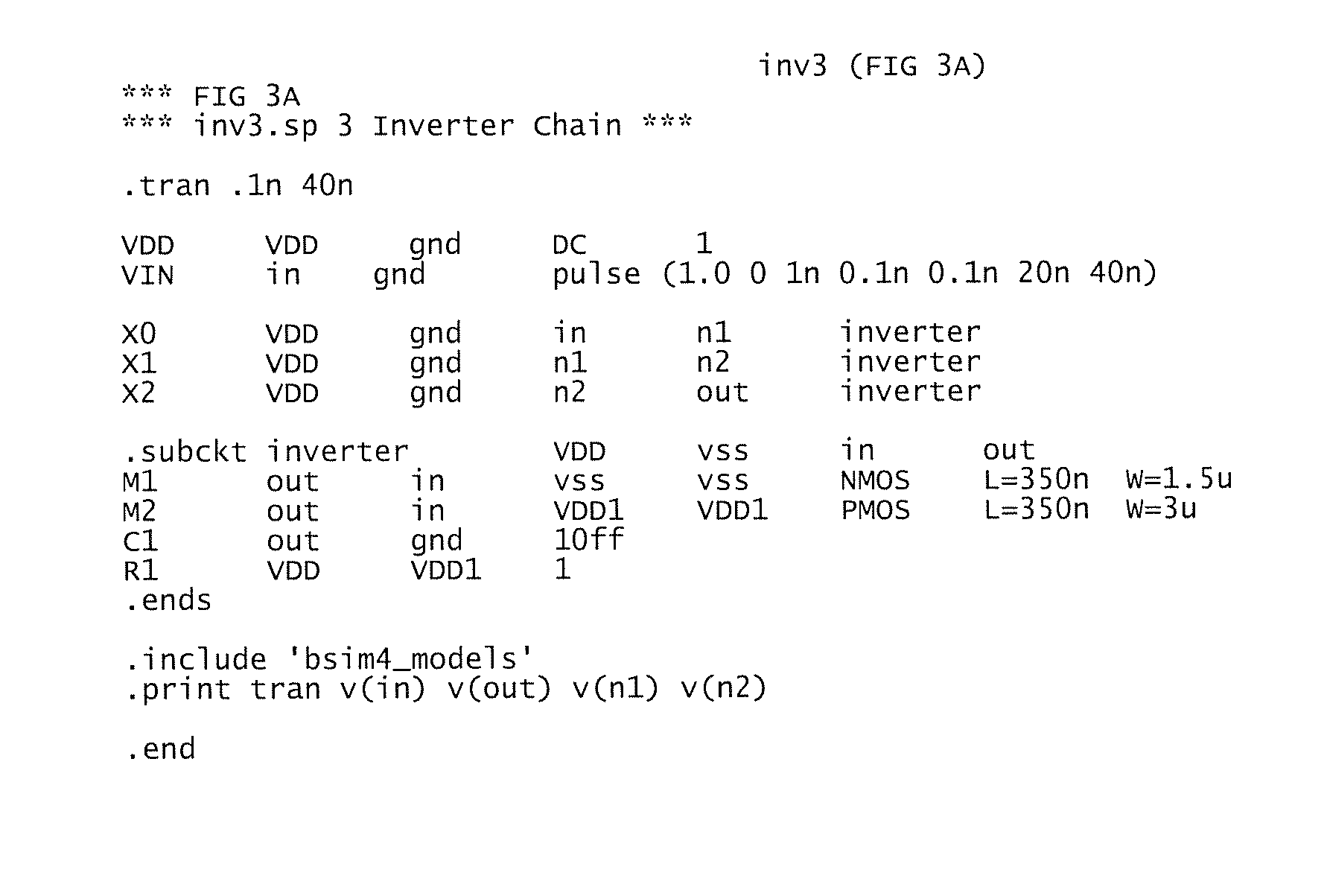
[0049]Hierarchical and flattened pre-layout and post-layout circuit descriptions or netlists are illustrated by way of examples in FIGS. 3A-3E, FIGS. 4-5, and FIGS. 6A-6B.

[0050]FIG. 3A shows a typical SPICE-compatible netlist of a 3-inverter circuit. The netlist describes a circuit that includes MOS transistors, resistors, and capacitors; the netlist contains a sub-circuit definition of an inverter provided in the .subckt directive, and serially connected instances X0, X1 and X2 of the inverter sub-circuit, each of which contains two MOS transistors, ...


PUM


Abstract

A method for reducing the size of post-layout circuit simulation output waveform database without a loss of essential information and accuracy. The reduced waveform database requires significantly less storage than the typical waveform database for post-layout simulation, thereby improving the time required for a waveform tool to access, and for a user to navigate, the post-layout simulation results. The method therefore greatly improves designer productivity during circuit verification and debugging phases. The method can be carried out in a preprocessor to a circuit simulator, in a post-processor to a circuit simulator, or may be directly built into a circuit simulator. The method is applicable to any post-layout netlists with schematic node names or circuit element names.

Description

BACKGROUND OF THE INVENTION[0001]1. Field of the Invention[0002]The present invention relates to post-layout circuit simulation. In particular, the present invention relates to techniques that reduce the size of a post-layout circuit simulation output waveform database, without loss of essential information and accuracy.[0003]2. Discussion of the Related Art[0004]As the feature sizes of an integrated circuit (IC) decrease, and as circuit density and performance increase, circuit simulation has become a critical aspect of ensuring that the IC meets requirements. However, as IC technology continues to advance, circuit simulation continues to require greater computing resources and time. Consequently, circuit verification and debugging based on circuit simulation results have become the bottleneck in the design process of ICs.[0005]In the IC design flow, a pre-layout circuit simulation primarily verifies circuit functionality and performs a first-pass circuit optimization. Because pre-...

Claims


Application Information

Patent Timeline
IPC IPC(8): G06F17/50
CPCG06F17/5036G06F17/5045G06F30/367
Inventor TUAN, JEH-FU
Owner ANALOG DESIGN AUTOMATION
Why Eureka
Try Eureka