Ultra-thin, planar, plasmonic metadevices

a meta-device, ultra-thin technology, applied in the field of planar devices, can solve the problems of limited phase control, difficult to make devices with a large aperture and a short focal length, and limited light bending strength in such a system, so as to achieve the effect of controlling the focal length of each devi

Active Publication Date: 2015-10-29
PURDUE RES FOUND INC
View PDF4 Cites 21 Cited by
  • Summary
  • Abstract
  • Description
  • Claims
  • Application Information

AI Technical Summary

Benefits of technology

[0008]The openings within each device are designed such that the polarization (either x- or y-) does not affect the focusing or diffracting ability or properties of the device, allowing each device to be polarization-independent. Additionally, the focal length of each device can be controlled by adjusting the wavelength of the incident light. In general, however, the focal length of the device is between one and fifteen micrometers, allowing for the focusing or diffracting of incident light in very small areas.

Problems solved by technology

The strength of the light bending in such a system is therefore limited by the refractive index of a given dielectric.
Fabrication challenges are also paramount, as it is very difficult to make devices with a large aperture and a short focal length.
Nevertheless, those designs suffer from limited phase control, which restricts their minimum sizes and thicknesses: either the size of the device cannot be further reduced because the design is based on the diffraction of the light through transparent / opaque regions, or the thickness of the device must be comparable to the operational wavelength because the phase change is obtained by light propagating inside the lens material.

Method used


Image

  • Ultra-thin, planar, plasmonic metadevices
  • Ultra-thin, planar, plasmonic metadevices
  • Ultra-thin, planar, plasmonic metadevices

Examples


Embodiment Construction

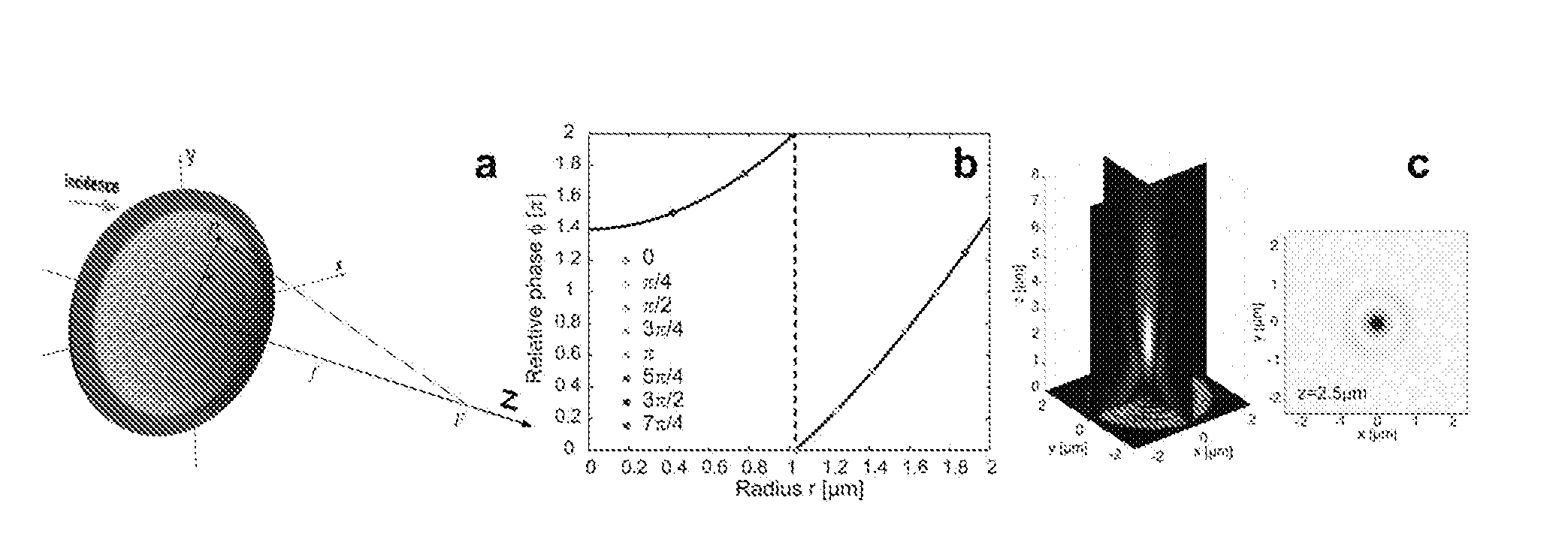
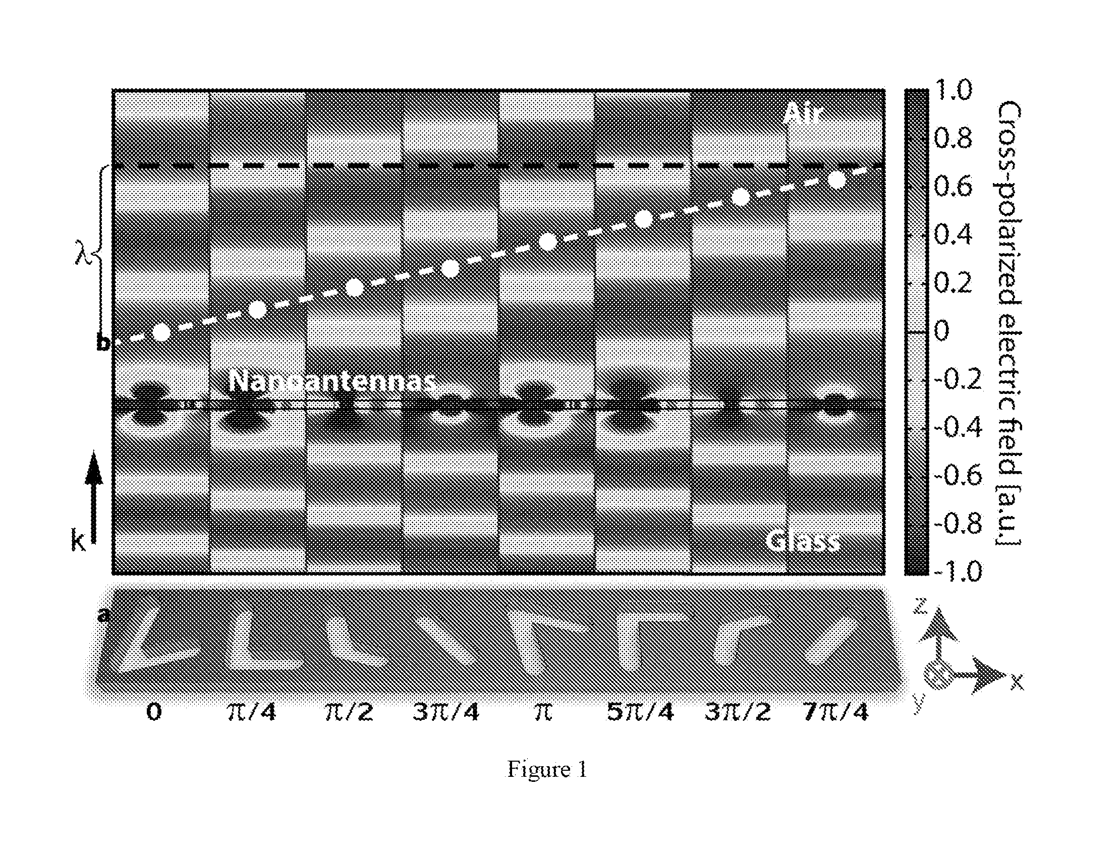
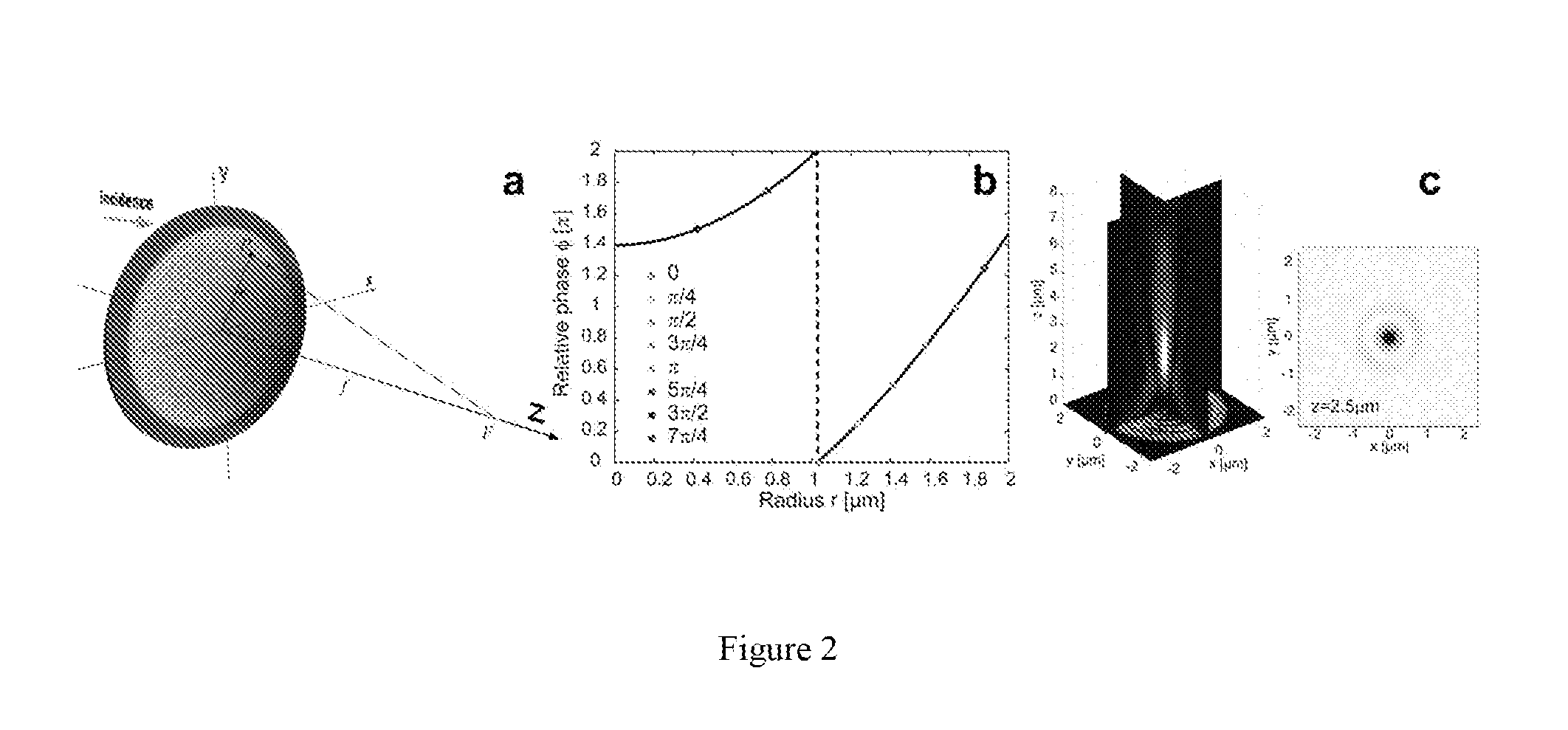
[0016]In contrast to conventional nano-antennas, the presently claimed device and method employ an inverted design built on Babinet's principle. That is, instead of metallic nano-antennas the claimed invention uses a set of similarly shaped nano-voids (Babinet-inverted, or complementary, nanoantennas) milled, or perforated, in a thin metallic film. Such a design provides a significantly higher signal-to-noise ratio. The nano-voids are arranged in arrays, or patterns, to create a planar plasmonic metadevice in order to much more efficiently focus or diffract (i.e. change the phase and the magnitude of) the incident light. In contrast to the near-IR device with focusing distances on the centimeter scale, the presently claimed plasmonic metadevices are very small in size (a few micrometers). Additionally, the present metadevices have an extremely strong focusing ability, with focal lengths of only a few micrometers and very large effective numerical apertures (NAs). Additionally, the m...


PUM


Abstract

An ultra-thin planar device is used for arbitrary waveform formation on a micrometer scale, regardless of the incident light's polarization. Patterned perforations are made in a 30 nm-thick metal film, creating discrete phase shifts and forming a desired wavefront of cross-polarized, scattered light. The signal-to-noise ratio of these devices is at least one order of magnitude higher than current metallic nano-antenna designs. The focal length of a lens built on such principle can also be adjusted by changing the wavelength of the incident light. All proposed embodiments can be embedded, for example, on a chip or at the end of an optical fiber.

Description

CROSS-REFERENCE TO RELATED APPLICATIONS[0001]This patent application claims priority to, and incorporates fully by reference, U.S. Provisional Patent Application No. 61 / 696,643, filed Sep. 4, 2012, and U.S. Provisional Patent Application No. 61 / 722,669, filed Nov. 5, 2012.STATEMENT REGARDING FEDERALLY SPONSORED RESEARCH[0002]This invention was made with government support under N00014-10-1-0942 awarded by Navy Office of Naval Research; FA9550-12-1-0024 awarded by United States Air Force Office of Scientific Research; DMR1120923 awarded by National Science Foundation, and UES-875-060-001 awarded by United States Air Force Research Laboratory. The government has certain rights in the invention.FIELD OF THE INVENTION[0003]This invention relates to planar devices for arbitrary waveform formation and in particular to those devices used in compact optical systems and other micro-scale technologies.BACKGROUND OF THE INVENTION[0004]The convergence or divergence of an optical beam in a tradi...

Claims


Application Information

Patent Timeline
Patent Type & Authority Applications(United States)
IPC IPC(8): G02B5/00G02B1/00
CPCG02B5/008Y10S977/834B82Y20/00G02B1/002
Inventor SHALAEV, VLADIMIRKILDISHEV, ALEXANDERNI, XINGJIEISHII, SATOSHI
Owner PURDUE RES FOUND INC
Why Eureka
Try Eureka