Gate Driver for Narrow Bezel LCD

a technology of liquid crystal display and driver, which is applied in the field of flat panel display, can solve the problems of increasing the rc effect to consume much energy and fail, and achieve the effect of reducing the rc

Active Publication Date: 2015-10-29
TCL CHINA STAR OPTOELECTRONICS TECH CO LTD
View PDF5 Cites 32 Cited by
  • Summary
  • Abstract
  • Description
  • Claims
  • Application Information

AI Technical Summary

Benefits of technology

[0020]Compared with the prior art, the gate driver in the present invention simplifies a circuit structure by effectively compounding the pull-down holding circuit and signals to achieve a design for ultra-narrow bezel gate driver. In addition, It effectively lessens voltage offset at the second node P(N) and prolongs GOA circuit operating time to prolongs LCD life when the seventh transistor of the first pull-down holding circuit adopts equivalent diode connection. At last, it reduces RC delay to efficiently lower power-consumption to more effectively decrease LCD energy-consumption when amount of transistors and signals of the first and the second pull-down holding circuits decreases.

Problems solved by technology

There are faults for conventional GOA circuit that too many TFTs and signal lines in a circuit for a disadvantage of a narrow or even none bezel display device and inevitably increasing RC effect to consume much energy to fail to meet a demand of green environment in the future.

Method used


Image

  • Gate Driver for Narrow Bezel LCD
  • Gate Driver for Narrow Bezel LCD
  • Gate Driver for Narrow Bezel LCD

Examples


first embodiment

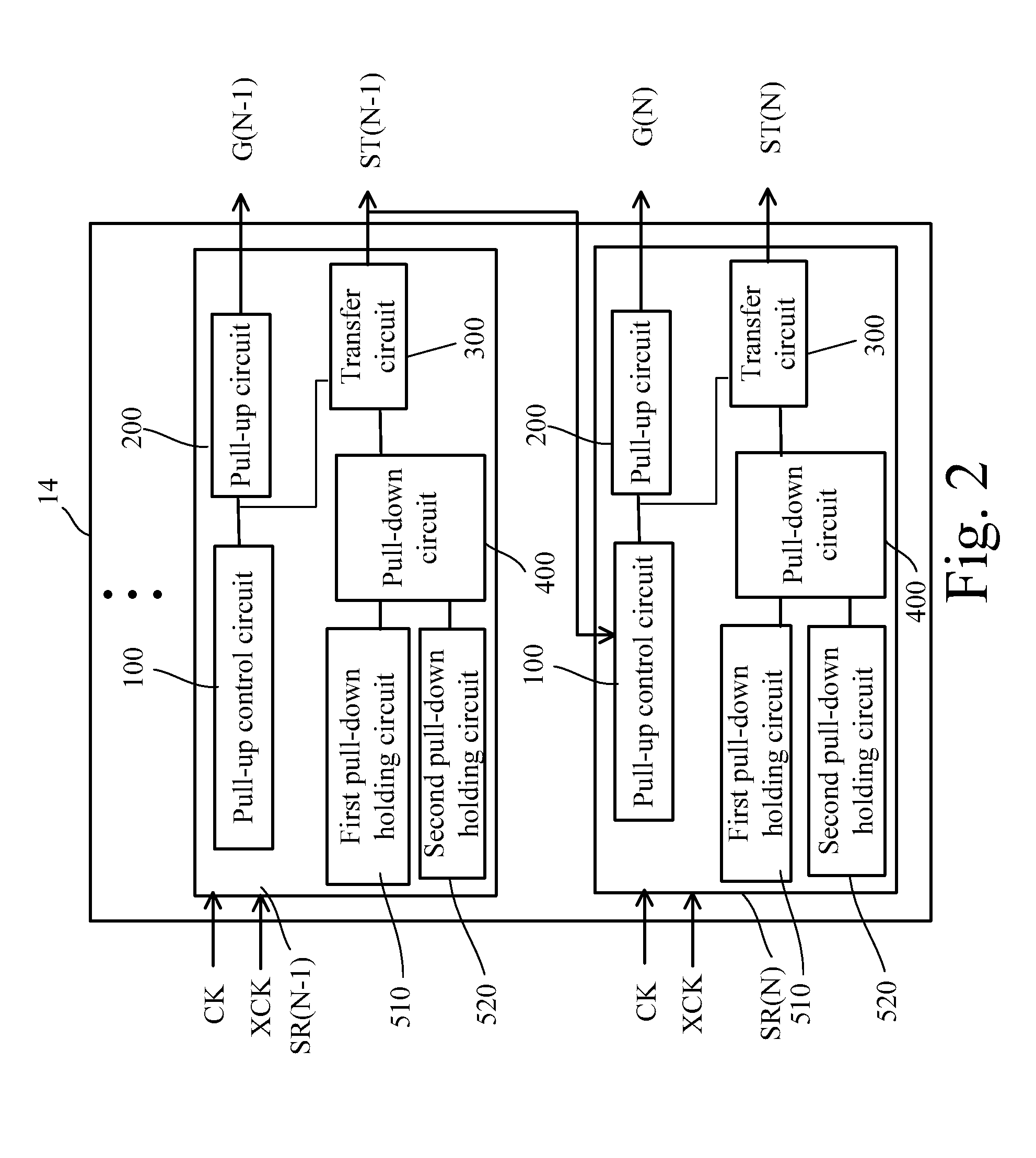
[0047]Refer to FIG. 3A, FIG. 3A is a circuit diagram of the shift register unit SR(N) shown in FIG. 2 according to the present invention. The pull-up circuit 200 may be a first transistor T1 whose a gate coupled to the first node Q(N), a source coupled to the first clock signal CK, a drain coupled to an output end G(N) for providing signal pulses to the output end G(N) based on the first clock signal CK. The transfer circuit 300 may be a second transistor T2 whose a gate coupled to the first node Q(N), a source coupled to the first clock signal CK, a drain coupled to a driving signal end ST(N) for providing driving signal pulses to the driving signal end ST(N) based on the first clock signal CK. The pull-up control circuit 100 is able to a third control circuit T3 whose a gate coupled to an output signal end G(N−1) of the previous one shift register unit SR(N−1), a drain coupled to the first node Q(N) for conducting the pull-up circuit 200 according to driving signal pulses of the p...

second embodiment

[0053]Please refer to FIG. 4A and FIG. 4B. FIG. 4A is a circuit diagram of the shift register unit shown in FIG. 2 according to the present invention. FIG. 4B is timing diagram of input signals, output signals, and voltages applied on nodes illustrated in FIG. 4A. The elements of the shift register unit SR(N) in FIG. 4A have the same labeled number with those of the shift register unit SR(N) in FIG. 3A have the identical operating principles, and no further description is demonstrated. A difference between the FIG. 4A and FIG. 3A is that the pull-down circuit 400 further comprises a sixteenth transistor T16, and the connections of the fifteenth transistor T15 and the sixteenth transistor T16 are not identical. A gate and a source of the fifteenth transistor T15 are respectively coupled to the driving signal end ST(n+1) of the next one shift register unit SR(n+1) for each shift register unit and to the first node Q(N). A gate and a source of the sixteenth transistor T16 are both coup...

third embodiment

[0054]Please refer to FIG. 5A and FIG. 5B. FIG. 5A is a circuit diagram of the shift register unit shown in FIG. 2 according to the present invention. FIG. 5B is timing diagram of input signals, output signals, and voltages applied on nodes illustrated in FIG. 5A. The elements of the shift register unit SR(N) in FIG. 5A have the same labeled number with those of the shift register unit SR(N) in FIG. 3A have the identical operating principles, and no further description is demonstrated. A difference between FIG. 5A and FIG. 3A is that the gate of the seventh transistor T7 of the first pull-down holding circuit 510 is coupled to the second node P(N) so that it reduces cross line crosstalk between the first clock signal CK and the second clock signal XCK. Compared with FIG. 3B, the second node P(N) discharges more effectively according to waveform of the seventh transistor T7. The operation principle and achieving effect of the shift register unit SR(N) in FIG. 5A is identical to which...


PUM


Abstract

The present invention proposes a gate driver which simplifies a circuit structure by effectively compounding the pull-down holding circuit and signals to achieve a design for ultra-narrow bezel gate driver. In addition, It effectively lessens voltage offset at the second node and prolongs GOA circuit operating time to prolongs lifetime of the LCD when the seventh transistor of the first pull-down holding circuit adopts equivalent diode connection. At last, it reduces RC delay to efficiently lower power-consumption to more effectively decrease LCD energy-consumption when amount of transistors and signals of the first and the second pull-down holding circuits decreases.

Description

CROSS REFERENCE TO RELATED APPLICATION[0001]The present application is based on, and claims priority from, Chinese application number 201410177821.2, filed Apr. 29, 2014, the disclosure of which is hereby incorporated by reference herein in its entirety.BACKGROUND OF THE INVENTION[0002]1. Field of the Invention[0003]The present invention relates to a flat panel display field, more particularly, to a gate driver for a narrow bezel liquid crystal display (LCD).[0004]2. Description of the Prior Art[0005]It adopts Gate Driver On Array (GOA) circuit to arrange a gate driver in a thin film transistor (TFT) array substrate through a TFT-LCD array process to act a progressive scanning driving.[0006]The GOA circuit mainly consists of a pull-up circuit, a pull-up control circuit, a transfer circuit, a pull-down circuit, a pull-down holding circuit and a boost circuit for boosting potentials.[0007]The pull-up circuit mainly outputs input clock signals to the TFT gate as driving signals for an ...

Claims


Application Information

Patent Timeline
Patent Type & Authority Applications(United States)
IPC IPC(8): G09G3/36
CPCG09G3/3674G09G2310/0291G09G2310/0286G09G2330/021G11C19/28
Inventor XIAO, JUNCHENG
Owner TCL CHINA STAR OPTOELECTRONICS TECH CO LTD
Why Eureka
Try Eureka