Transparent electrically conductive substrate and manufacturing method thereof

a technology of transparent electrically conductive substrate and manufacturing method, which is applied in the direction of conductive layers on insulating supports, drying machines, lighting and heating apparatus, etc., can solve the problems of metal nanowires becoming, and achieve the effect of improving the anisotropy of the orientation sta

Active Publication Date: 2015-11-12
CAMBRIOS FILM SOLUTIONS CORP
View PDF1 Cites 13 Cited by
  • Summary
  • Abstract
  • Description
  • Claims
  • Application Information

AI Technical Summary

Benefits of technology

[0013]Accordingly, the aim of the present invention is to provide a technique for improving the anisotropy of transparent electrically conductive substrates that employ metallic nanowires. That is, the aim is to provide a technique whereby the metallic nanowires become oriented non-uniformly by modifying the orientation of the metallic nanowires such that there is no difference between the TD surface resistance (RTD) and the MD surface resistance (RMD).
[0033]The present invention improves the anisotropy of the state of orientation of metallic nanowires in a transparent electrically conductive substrate comprising a substrate film on which is provided a conductive stratum containing metallic nanowires. The present invention is able to provide a method of manufacturing a transparent electrically conductive substrate whose surface resistance exhibits almost no anisotropy, and a transparent electrically conductive substrate whose surface resistance exhibits almost no anisotropy, obtained by means of this method of manufacture. Thus transparent electrically conductive substrates according to the present invention are suitable for use in touch panel electrodes and the like in which the surface resistance is preferably isotropic.

Problems solved by technology

However, an issue with transparent electrically conductive substrates in which metallic nanowires are employed is that the long axis of the metallic nanowires becomes aligned with the film transport direction (transport direction=longitudinal direction=MD [machine direction]).

Method used


Image

  • Transparent electrically conductive substrate and manufacturing method thereof
  • Transparent electrically conductive substrate and manufacturing method thereof
  • Transparent electrically conductive substrate and manufacturing method thereof

Examples


embodiments

Embodiments 1-6

[0057]Coating liquid: Mixture of 0.10 wt % metallic nanowires (fibre length: 1 to 100 μm) and 99.90 wt % solvent (pure water).

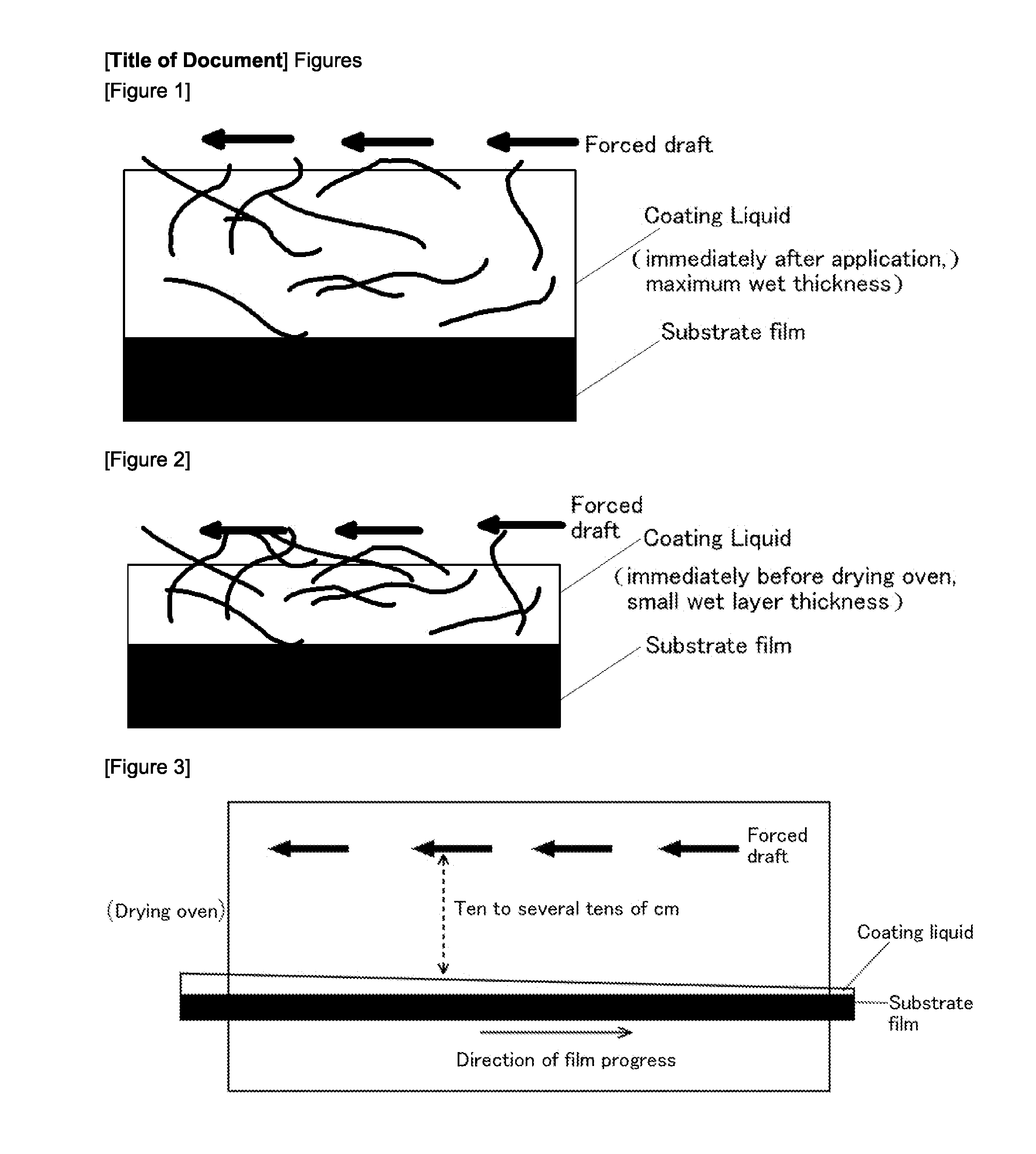
[0058]Application process: Using die coating method, the coating liquid is squeezed out from a slot die onto the substrate film which is being transported by roll conveyor. The thickness of the wet layer immediately after application is 15.0 μm.

Transport process: The substrate film onto which the coating liquid has been squeezed out is transported by roll conveyor to a drying oven.

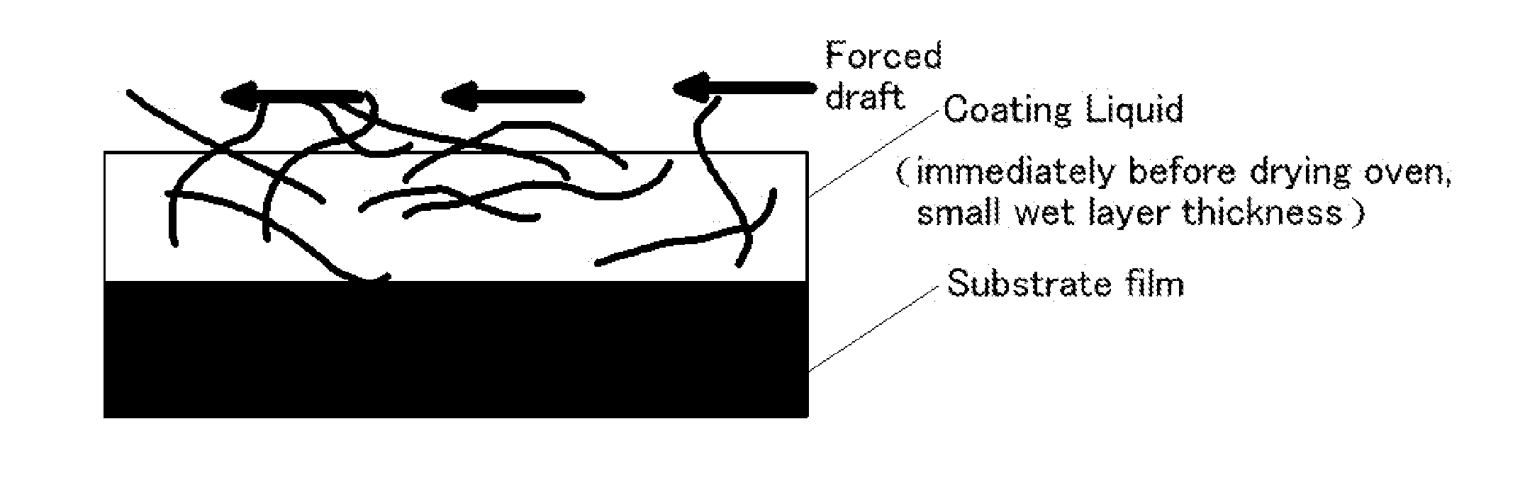
Drying process: Performed using a drying draft in a drying oven. Specifically, drying is performed by introducing drying air (40° C., 1 m / s) in the direction opposite to the direction of progress of the film, 30 cm above the surface of the wet layer. It should be noted that the drying draft was introduced in a zone in which a forced draft was not introduced from the TD. In other words, in the present embodiment a drying draft is not blown in zones in which a forced dr...

embodiments 7-9

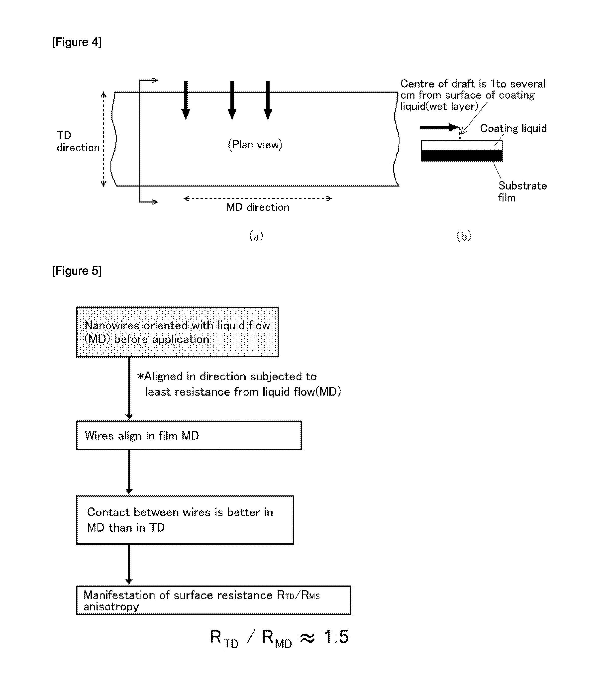
[0063]Experiments were next performed varying the speed of the draft from the TD. It should be noted that the proportion of metallic nanowires was 0.18%, and solvent (pure water) was 99.82%, the film transport speed was 10 m / s, and the draft from the TD was blown in the first and second zones. The results are shown in Table 4.

TABLE 4Embodiment7Embodiment 8Embodiment 9Wind speed (m / s)4.46.910.4Surface resistance (RTD)535151(Ω)Surface resistance (RMD)485459(Ω)RTD / RMD1.100.940.86

[0064]Improvements in RTD / RMD were observed by increasing the wind speed of the draft from the TD. Depending on the conditions, in some cases RMD even exceeded RTD (RTD / RMD was less than 1).

[0065]A transparent electrically conductive substrate was manufactured under the same conditions as in embodiment 8, with only the film transport speed returned to 15 m / s. RTD / RMD was 1.1. If the amount of reduction in the thickness of the wet layer is within the same range, then if a draft to modify the orientation of the n...


PUM

PropertyMeasurementUnit
thicknessaaaaaaaaaa
speedaaaaaaaaaa
temperatureaaaaaaaaaa

Abstract

[Problem] To improve the anisotropy of transparent electrically conductive substrates that employ metallic nanowires.[Means of overcoming the problem] Method of manufacturing a transparent electrically conductive substrate having an application process whereby a wet layer is formed by applying onto a substrate film a coating liquid comprising metallic nanowires dispersed in a solvent, and a drying process whereby the solvent contained in the abovementioned wet layer is removed by drying,characterised in that the abovementioned drying process includes a process whereby the orientation of the abovementioned metallic nanowires is altered by introducing a forced draft facing towards the substrate from a direction that is different from the longitudinal direction of the substrate film.

Description

TECHNICAL FIELD[0001]The present invention relates to a method of manufacturing a transparent electrically conductive substrate whose surface resistance exhibits almost no anisotropy, comprising a substrate film on which is provided a conductive stratum containing metallic nanowires in an unaligned state of orientation. In particular it relates to a method in which a coating fluid containing metallic nanowires is dried after having been applied onto the substrate, an orientation of the metallic nanowires is modified such that the metallic nanowires become oriented non-uniformly.BACKGROUND ART[0002]Transparent electrically conductive substrates are used in flat displays and touch panels, and electroluminescent devices and the like. Typical transparent electrically conductive materials are configured from a substrate film and a metal oxide such as tin-doped indium oxide (ITO), and typical manufacturing methods are vapour-phase film forming methods such as vacuum deposition methods, sp...

Claims


Application Information

Patent Timeline
Patent Type & Authority Applications(United States)
IPC IPC(8): B05D3/04B05D1/26
CPCB05D3/042Y10T428/249924B05D1/265B82Y30/00C09D5/02B22F7/04H01B1/02B05D3/0272B05D3/0413B05D7/04B05D1/26B05D2252/02B05D2601/28F26B21/004F26B2210/00B22F3/22B22F1/0547H10K30/82H01B5/14H01B13/00H01L31/022466
Inventor MISHIMA, TAKASHIGOTO, KEISUKEPSCHENITZKA, FLORIANWESTWATER, JONATHAN
Owner CAMBRIOS FILM SOLUTIONS CORP
Why Eureka
Try Eureka