Ceramic electronic component and manufacturing method therefor

Active Publication Date: 2015-11-12
MURATA MFG CO LTD
View PDF7 Cites 20 Cited by
  • Summary
  • Abstract
  • Description
  • Claims
  • Application Information

AI Technical Summary

Benefits of technology

[0027]According to an aspect of the present invention, the coating film can be selectively formed only on the ceramic part without carrying out glass coating or resin coating. Accordingly, the ceramic electronic component can be obtained who

Problems solved by technology

However, in the case of coating a ceramic surface of an electronic component with glass as in JP5-101910 A, there is a need for a firing step, thereby leading to an increase in manufacturing cost.
Moreover, it is not possible to form any film with positional selectivity, because the glass coating is provided (applied) over the entire surface of the electronic component.
Therefore, there is a need for a step of forming a glass coating film over the entire surface of the electronic component before the formation of external electrodes, and removing the glass coating film on end surfaces of the electronic component on which external electrodes are to be formed, and the manufacturing cost is thus increased.
However, in this case, there is a limit on the thickness of the glass coating film, and the management for mass production will become complicated.
In addition, in the case of coating a ceramic surface of an electronic co

Method used


Image

  • Ceramic electronic component and manufacturing method therefor
  • Ceramic electronic component and manufacturing method therefor
  • Ceramic electronic component and manufacturing method therefor

Examples


examples

1. Examples and Comparative Examples

[0102]Respective ceramic electronic components (varistors, multilayer ceramic capacitors, laminated coils, PTC thermistors, NTC thermistors, LTCC substrates) according to examples and comparative examples were prepared, and subjected to characterization.

2. Preparation of Examples and Comparative Examples

[0103](a) Examples 1 to 9

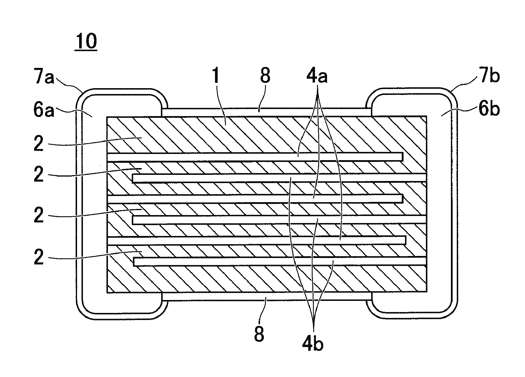
[0104]As shown in Table 1, the varistor 10 with the coating film 8 provided on the surface of the ceramic main body 1 was prepared by the manufacturing method [Method 1] according to the embodiment described previously.

[0105]As the resin-containing solution, a commercially available latex of a resin component dispersed in a solvent containing water was used with an etching promoting constituent added thereto, if necessary.

[0106]As the resin-containing solutions according to Examples 1 to 3, an acrylic resin (Trade Name: Nipol LX814A (from Zeon Corporation)) as the resin component was used through the adjustment of the pH to...


PUM

PropertyMeasurementUnit
Temperatureaaaaaaaaaa

Abstract

A ceramic electronic component that includes a ceramic main body, a coating film and external electrodes on the surface of the ceramic main body. The coating film is selectively formed on the surface of the ceramic main body by applying, to the surface of the ceramic main body, a resin-containing solution that etches the surface of the ceramic main body so as to ionize constituent elements of the ceramic main body. The coating film includes a resin and the constituent elements of the ceramic main body, which were ionized and deposited from the ceramic main body.

Description

CROSS REFERENCE TO RELATED APPLICATIONS[0001]The present application is a continuation of International application No. PCT / JP2014 / 051826, filed Jan. 28, 2014, which claims priority to Japanese Patent Application No. 2013-014482, filed Jan. 29, 2013, the entire contents of each of which are incorporated herein by reference.BACKGROUND OF THE INVENTION[0002]1. Field of the Invention[0003]The present invention relates to a ceramic electronic component and a method for manufacturing the component.[0004]2. Description of the Related Art[0005]The ceramics for use in electronic components may be likely to be weakened against chemical erosion by acid or alkali, and also undergo a decrease in mechanical strength of themselves, because of improvements in material due to the sophisticated functions of the electronic components.[0006]Therefore, as measures against this situation, techniques have been proposed for coating ceramic surfaces of electronic components with glass as in JP5-101910 A, o...

Claims


Application Information

Patent Timeline
IPC IPC(8): H01G2/12C23C28/00H01C7/10H01G4/12H01F27/28H01G4/005H01C7/04H01F41/00H01C17/00H01G4/30H01F27/23C25D7/00H01C7/02
CPCH01G2/12C25D7/00C23C28/00H01C7/10H01G4/12H01F27/2804H01F2027/2809H01C7/04H01F41/00H01C17/00H01G4/30H01F27/23H01G4/005H01C7/02H01C17/02H01G4/224H01C7/003H01C7/1006H01C7/102H01G2/103C25D5/54C25D5/56C23C18/1641C23C18/1882
Inventor INOUE, MITSUNORIMORI, TOMOHIKO
Owner MURATA MFG CO LTD
Why Eureka
Try Eureka