Touch panel

a technology of touch panel and detection sensitivity, which is applied in the field of touch panel, can solve the problems of reducing the detection sensitivity of the touch panel in some cases, and achieve the effect of improving the detection sensitivity of the touch panel and high reliability

Inactive Publication Date: 2015-12-03
SEMICON ENERGY LAB CO LTD
View PDF11 Cites 105 Cited by
  • Summary
  • Abstract
  • Description
  • Claims
  • Application Information

AI Technical Summary

Benefits of technology

[0025]One embodiment of the present invention can improve the detection sensitivity of a touch panel. Alternatively, a thin touch panel can be provided. Alternatively

Problems solved by technology

In a touch panel where a capacitive touch sensor is provided so as to overlap with the display surface side of a display panel, when the distance between a pixel or a wiring of the display panel and an electrode or a wiring of the

Method used


Image

  • Touch panel
  • Touch panel
  • Touch panel

Examples


embodiment 1

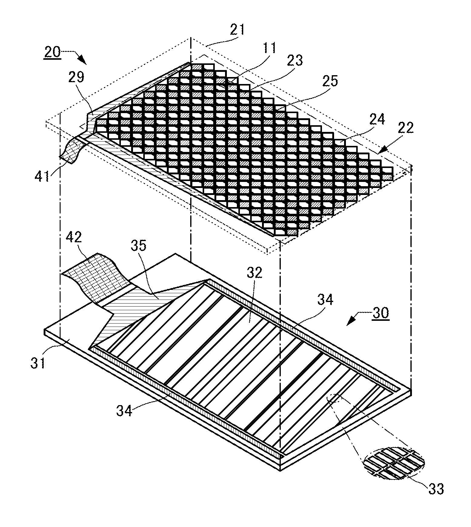
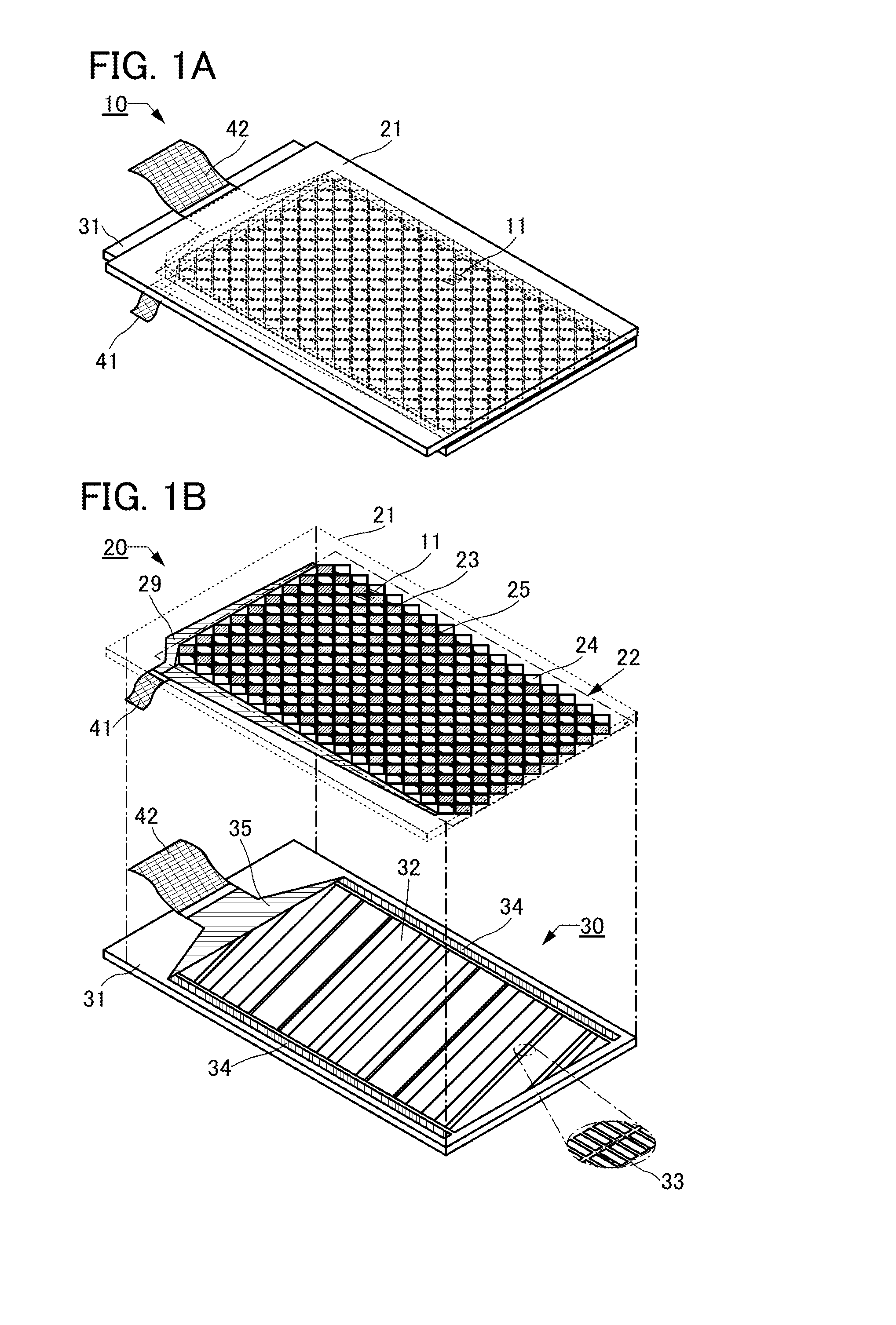
[0054]In this embodiment, a structure example of a touch panel of one embodiment of the present invention will be described with reference to drawings. In the description below, a capacitive touch sensor is used as a touch sensor of a touch panel.

[0055]Note that in this specification and the like, a touch panel has a function of displaying or outputting an image or the like on or to a display surface and a function of a touch sensor capable of sensing contact or proximity of an object such as a finger or a stylus on or to the display surface. Therefore, the touch panel is an embodiment of an input / output device.

[0056]In this specification and the like, a structure in which a connector such as a flexible printed circuit (FPC) or a tape carrier package (TCP) is attached to a substrate of a touch panel, or a structure in which an integrated circuit (IC) is directly mounted on a substrate by a chip on glass (COG) method is referred to as a touch panel module or simply referred to as a t...

embodiment 2

[0214]In this embodiment, an example of a method for operating the touch panel of one embodiment of the present invention is described with reference to drawings.

[Example of Sensing Method of Sensor]

[0215]FIG. 16A is a block diagram illustrating the structure of a mutual capacitive touch sensor. FIG. 16A illustrates a pulse voltage output circuit 601 and a current sensing circuit 602. Note that in FIG. 16A, six wirings X1 to X6 represent the electrodes 621 to which a pulse voltage is applied, and six wirings Y1 to Y6 represent the electrodes 622 that detect changes in current. FIG. 16A also illustrates a capacitor 603 that is formed where the electrodes 621 and 622 overlap with each other. Note that functional replacement between the electrodes 621 and 622 is possible.

[0216]The pulse voltage output circuit 601 is a circuit for sequentially applying a pulse voltage to the wirings X1 to X6. By application of a pulse voltage to the wirings X1 to X6, an electric field is generated betwe...

embodiment 3

[0229]In this embodiment, electronic appliances and lighting devices that can be fabricated according to one embodiment of the present invention will be described with reference to FIGS. 18A to 18G and FIGS. 19A to 19I.

[0230]The touch panel of one embodiment of the present invention has flexibility. Therefore, a touch panel of one embodiment of the present invention can be used in electronic appliances and lighting devices having flexibility. Furthermore, according to one embodiment of the present invention, electronic appliances and lighting devices having high reliability and resistance against repeated bending can be manufactured.

[0231]Examples of electronic appliances include a television set (also referred to as a television or a television receiver), a monitor of a computer or the like, a digital camera, a digital video camera, a digital photo frame, a mobile phone (also referred to as a mobile phone device), a portable game machine, a portable information terminal, an audio r...


PUM


Abstract

To increase the detection sensitivity of a touch panel, provide a thin touch panel, provide a foldable touch panel, or provide a lightweight touch panel. A display element and a capacitor forming a touch sensor are provided between a pair of substrates. Preferably, a pair of conductive layers forming the capacitor each have an opening. The opening and the display element are provided to overlap each other. A light-blocking layer is provided between a substrate on the display surface side and the pair of conductive layers forming the capacitor.

Description

BACKGROUND OF THE INVENTION[0001]1. Field of the Invention[0002]One embodiment of the present invention relates to a touch panel.[0003]Note that one embodiment of the present invention is not limited to the above technical field. One embodiment of the invention disclosed in this specification and the like relates to an object, a method, or a manufacturing method. One embodiment of the present invention relates to a process, a machine, manufacture, or a composition of matter. Specifically, examples of the technical field of one embodiment of the present invention disclosed in this specification include a semiconductor device, a display device, a light-emitting device, a power storage device, a memory device, an electronic appliance, a lighting device, an input device, an input / output device, a method for driving any of them, and a method for manufacturing any of them.[0004]In this specification and the like, a semiconductor device generally means a device that can function by utilizi...

Claims


Application Information

Patent Timeline
IPC IPC(8): G06F3/044G06F3/0488G06F15/02G06F3/041G06F3/045
CPCG06F3/0412G06F3/045G06F15/0216G06F3/0488G06F3/044G06F2203/04102G06F2203/04104G06F2200/1633G06F2203/04808G06F2203/04101G06F2203/04111G06F2203/04112G06F1/1618G06F1/1652G06F1/1677G06F3/04166G06F3/0446G06F3/0445H10K59/40H10K77/111G06F2203/04103Y02E10/549
Inventor KUSUNOKI, KOJIMIYAKE, HIROYUKIWATANABE, KAZUNORI
Owner SEMICON ENERGY LAB CO LTD
Why Eureka
Try Eureka