Circuit Board Having Interposer Embedded Therein, Electronic Module Using Same, and Method for Manufacturing Same

a technology of interposer and electronic module, which is applied in the direction of final product manufacturing, sustainable manufacturing/processing, and semiconductor/solid-state device details, etc., can solve the problems of not being able to realize, and achieve the effect of improving integration, optimal 3d package structure, and easy disposing of interposers in required sections

Inactive Publication Date: 2015-12-10
HANA MICRON
View PDF0 Cites 43 Cited by
  • Summary
  • Abstract
  • Description
  • Claims
  • Application Information

AI Technical Summary

Benefits of technology

[0008]As described above, the following effects may be expected according to a configuration of the present invention.
[0009]Firstly, since an interposer being a semiconductor is partly coupled to a circuit board being an insulator, there are effects that the mechanical strength of the entire circuit board is maintained as it is and degree of integration is enhanced through the fine-pitch function of the interposer.
[0010]Secondly, since the interposer is disposed on a carrier, an insulating material is molded and the interposer is exposed through a polishing process, there is an effect that it is possible to easily dispose the interposer in a required section.
[0011]Thirdly, since a semiconductor chip having a logic function is embedded along with the interposer, it is possible to realize a wafer level package.
[0012]Fourthly, since semiconductor chips having a memory function are disposed on the circuit board in a vertically stacked manner and these are electrically connected through the through-electrode of the interposer, it is possible to realize an optimal 3D package structure.

Problems solved by technology

The laser drill process is useful for forming a through hole having a certain pitch or more but it is not longer possible to realize the fine pitch of the through hole with the laser drill process because the circuit board formed of the insulating material also needs degree of integration in light of the reduction of a design rule and the general miniaturization trend of a product.

Method used


Image

  • Circuit Board Having Interposer Embedded Therein, Electronic Module Using Same, and Method for Manufacturing Same
  • Circuit Board Having Interposer Embedded Therein, Electronic Module Using Same, and Method for Manufacturing Same
  • Circuit Board Having Interposer Embedded Therein, Electronic Module Using Same, and Method for Manufacturing Same

Examples


Embodiment Construction

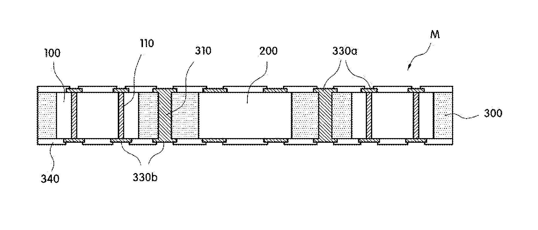
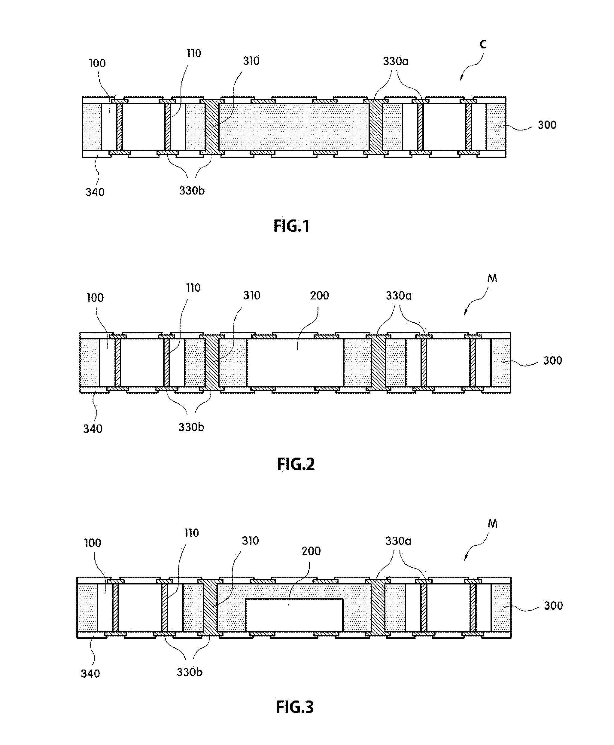
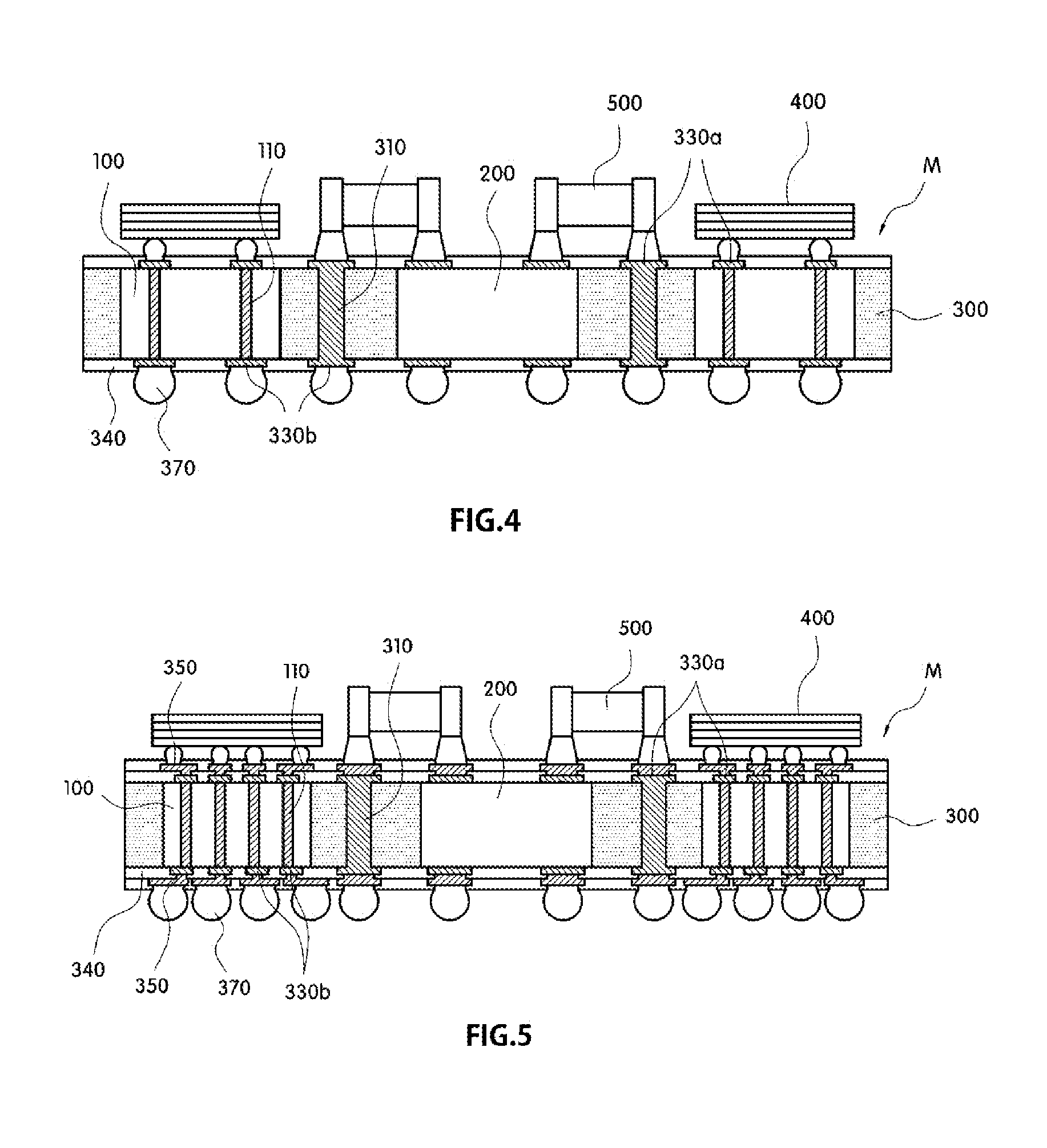
[0018]The advantages and features of the present invention, and implementation methods thereof will be clarified through the following embodiments described with reference to the accompanying drawings. The present invention may, however, be embodied in different forms and should not be construed as limited to the embodiments set forth herein. Rather, these embodiments are provided to make this disclosure complete and fully convey the scope of the present invention to a skilled in the art. Further, the present invention is only defined by the scopes of claims. In the drawings, the size and relative size of layers and regions may be exaggerated for the clarification of description. Like reference numerals throughout the disclosure refer to like components.

[0019]Embodiments described in the disclosure are described with reference to plane views and cross-sectional views that are ideal, schematic diagrams of the present invention. Thus, the forms of exemplary views may vary depending on...


PUM

PropertyMeasurementUnit
aspect ratioaaaaaaaaaa
depthaaaaaaaaaa
conductiveaaaaaaaaaa

Abstract

The present invention relates to a circuit board having an interposer embedded therein, including: an interposer, the top side and back side of which are electrically connected by a first through-electrode; and a molding member having the interposer embedded therein and the top side and back side of the interposer exposed. According to the present invention, the molding member of an insulator and the interposer of a semiconductor can be appropriately selected and coupled according to the required fine pitch of a through-hole, and the interposer is molded on substantially the same level as a semiconductor chip, and thus no additional process for embedding the interposer needs to be added.

Description

TECHNICAL FIELD[0001]The present invention relates to a circuit board having an interposer embedded therein relevant to a fan-out wafer level package (WLP), and a manufacturing method thereof, and more particularly, to a circuit board having an interposer embedded therein that maintains the advantage of a fan-out insulating substrate and improves degree of integration of a circuit board, by applying a silicon interposer to only some sections requiring a fine-pitch through hole of a circuit board formed of an insulating material because a molding member being an insulator and an interposer being a semiconductor are coupled, and a manufacturing method thereof.[0002]Also, the present invention relates to an electronic module using the circuit board having the interposer embedded therein and a manufacturing method thereof and more particularly to, an electronic module that has a semiconductor chip having a logic function embedded in the circuit board and has a semiconductor chip having ...

Claims


Application Information

Patent Timeline
Patent Type & Authority Applications(United States)
IPC IPC(8): H05K1/14H05K1/18H05K3/40H05K3/18H05K3/30H05K3/32H05K1/11H05K3/26
CPCH05K1/14H05K1/115H05K1/181H05K3/26H05K3/181Y10T29/49149H05K3/32H05K3/4038H05K2201/10159Y10T29/49131H05K3/303H01L21/486H01L21/568H01L23/147H01L23/5384H01L24/19H01L24/96H01L25/0652H01L25/105H01L25/16H01L2224/0401H01L2224/04105H01L2224/12105H01L2224/16227H01L2224/16235H01L2224/2518H01L2924/15311H01L2924/181H01L2924/19104H01L2924/19105H05K1/185H05K3/4602H05K2201/10378H05K2201/1053H05K2201/10636H05K2201/10674H05K2203/0191H05K2203/1469Y02P70/50H01L2924/00H01L23/64
Inventor OCK, JIN YOUNG
Owner HANA MICRON
Why Eureka
Try Eureka