Margin tool for double data rate memory systems

a memory system and data rate technology, applied in the field of circuits, can solve the problems of low phase-locked loop (“pll”) jitter, signal integrity of ddr memories, and increasing criticality of fast register propagation delay times

Active Publication Date: 2015-12-17
NXP USA INC
View PDF7 Cites 14 Cited by
  • Summary
  • Abstract
  • Description
  • Claims
  • Application Information

AI Technical Summary

Problems solved by technology

The higher speed of DDR memories makes signal integrity, low phase-locked loop (“PLL”) jitter, and fast register propagation delay times increasingly critical.
Thus, given these high clock rates and fast edge speeds, timing considerations become challenging; it is often the case that timing skews vary greatly from one system implementation to another, especially for systems with larger amounts of memory and a greater overall width of the memory bus.
In other words, the high speeds of DDR memories, and the very short valid data windows of DDR data, pose significant challenges when the memory controller is then implemented on a printed circuit board (“PCB”) with the associated memories and other integrated circuit chips.
The speeds at which the memory controller must reliably operate make the PCB layout challenging for the engineers and designers of such system boards.
These difficulties arise not from a functionality issue, but from the physical realities of working with valid data windows that are well within the magnitude of signal propagation delays.
These timing requirements are further complicated by the variation in logic speed over process, temperature, and voltage variations associated with the particular PCB on which the memory controller and DDR memories are implemented.
A problem with such training sequences is that they were designed and implemented into the memory controller when it was manufactured to operate under a limited set of parameters, which cannot take into account variations and / or deviations from such predetermined parameters when the PCB manufacturer integrates the memory controller with the DDR memories and other circuitry onto the PCB.
Furthermore, such training techniques may not take into account all of the process and operating variations under which the PCB experiences in the field by the ultimate customers.
For example, it is not practical to design such training sequences within the memory controller to incorporate wide and extreme variations in operating conditions of the final computing device while also striving to ensure that the memory controller is able to transfer data to / from the memory devices at the desired high speeds.

Method used


Image

  • Margin tool for double data rate memory systems
  • Margin tool for double data rate memory systems
  • Margin tool for double data rate memory systems

Examples


Embodiment Construction

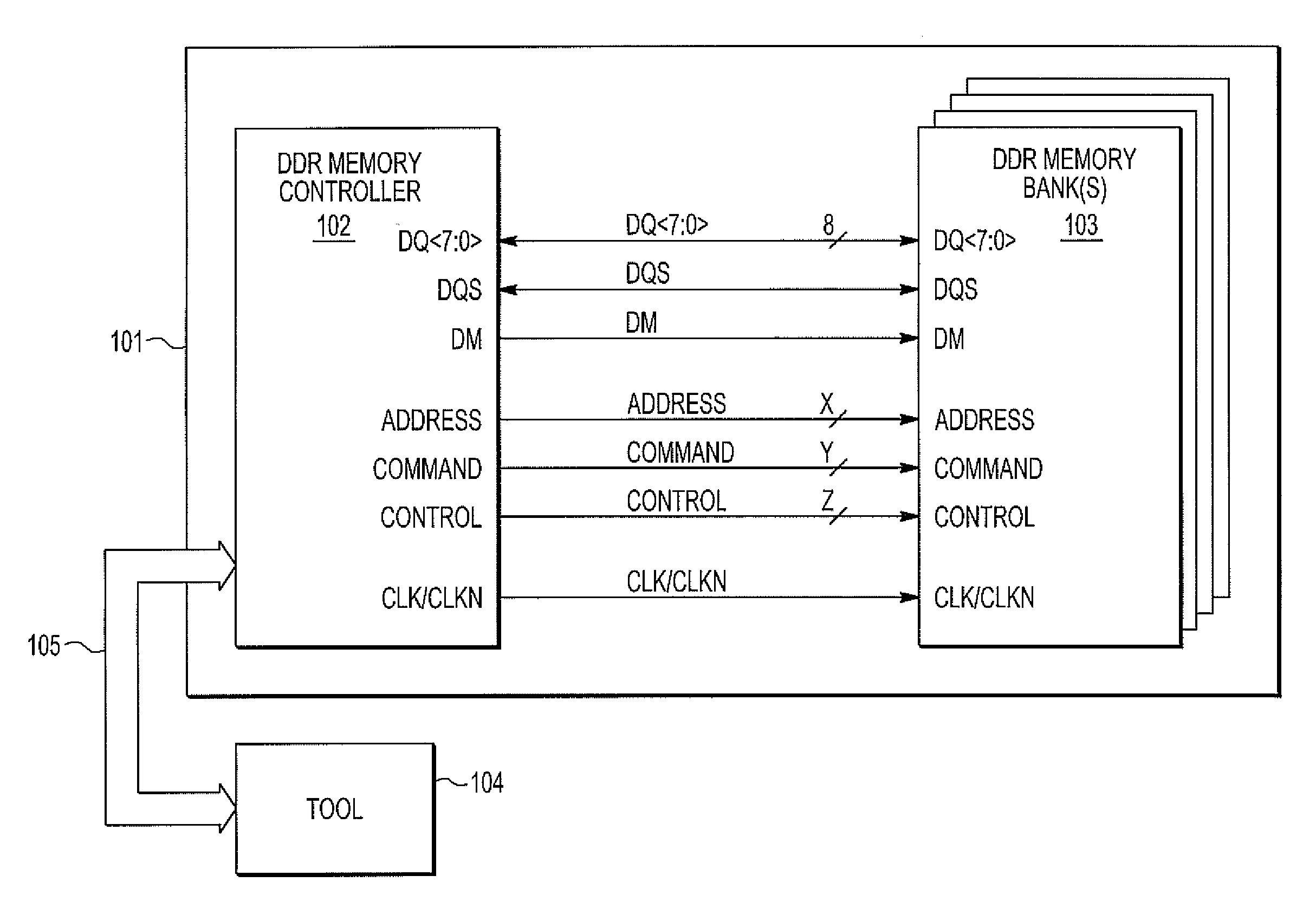
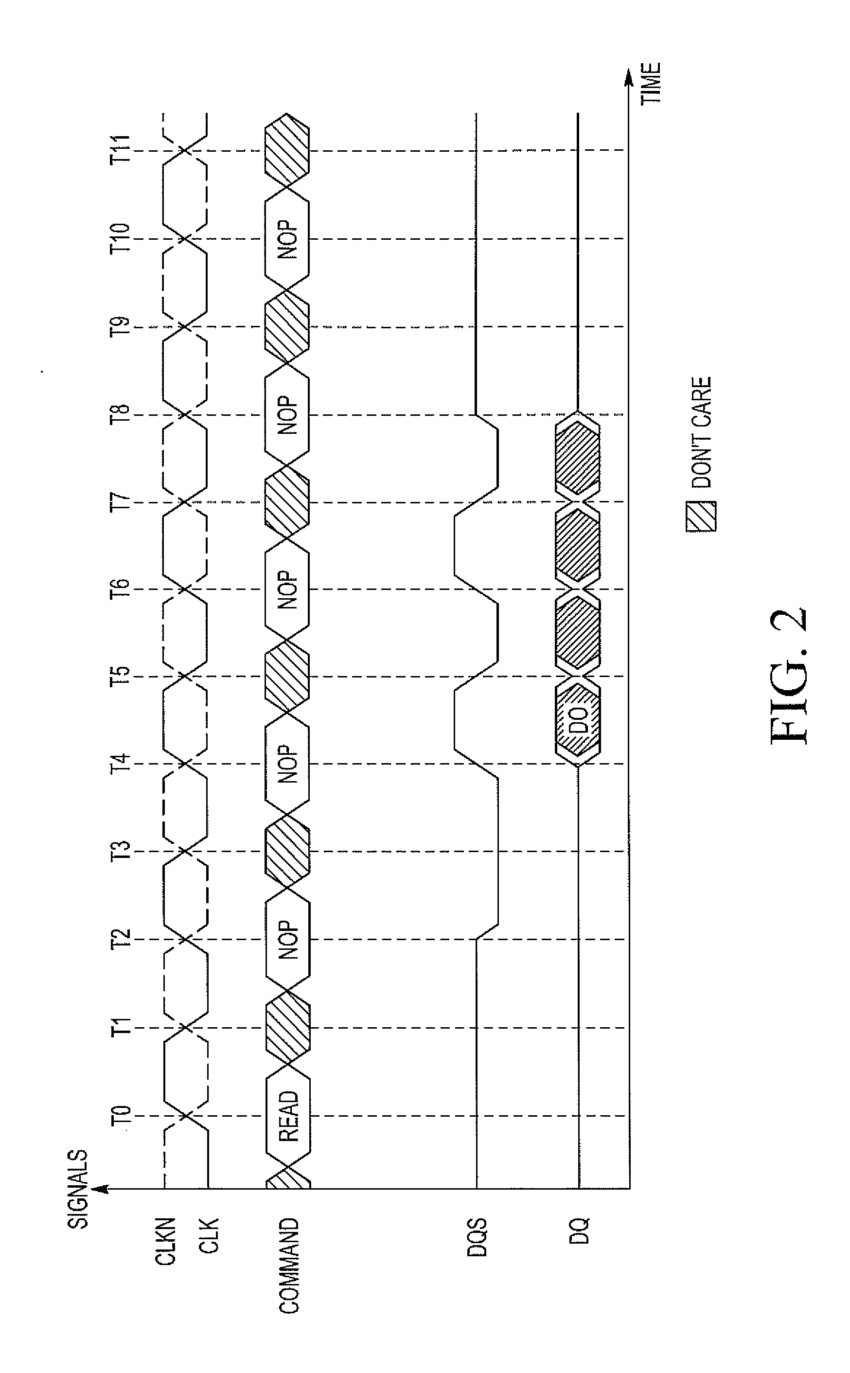
[0012]In a typical non-DDR memory system, both the memory controller and memory transmit or capture data in response to a single system clock. Compared to single data rate (“SDR”) DRAM, the DDR DRAM interface makes higher transfer rates possible by more strict control of the timing of the electrical data and clock signals. However, implementations often have to use schemes such as phase-locked loops and self-calibration to reach the required timing accuracy. The interface uses double pumping (transferring data on both the rising and falling edges of the clock signal) to lower the clock frequency. The name “double data rate” refers to the fact that a DDR DRAM with a certain clock frequency achieves nearly twice the bandwidth of a SDR DRAM running at the same clock frequency, due to this double pumping.

[0013]As memory designers have moved to a DDR implementation of such systems, they achieved a 2× effective increase in the bit rate of the system. However, this effectively cut the vali...


PUM


Abstract

A tool for testing a double data rate (“DDR”) memory controller to ensure that data strobe transitions are aligned with data eyes to achieve a desired data integrity during data transfers between the memory controller and the memories. After the memory controller completes its training sequence during the initialization process, the tool sweeps the data strobe transition across the data eye. At each timing step during the sweep, several tests may be conducted to check for integrity of functionality. The tool thus generates a pass / fail margin table. The locations of the data strobe transitions selected by the memory controller during its previously run training sequence are then added to this tool-generated margin table. The result is essentially a pseudo data eye, reconstructed including the data strobe transition with the data eye. An inspection of the location of the data strobe transition with the data eye may be utilized to show the range of timing steps available before the data strobe transition would fail to capture valid data from the incoming data eye.

Description

TECHNICAL FIELD[0001]This application relates in general to circuits that interface with dynamic memories, and in particular double data rate (“DDR”) memories.BACKGROUND INFORMATION[0002]Double data rate (“DDR”) dynamic random-access (“DRAM”) memory (hereinafter referred to as “DDR memory”) is a class of memory integrated circuits used in computing systems. DDR memory uses a clocking technique whereby two data bits are transferred per clock cycle, or once every clock edge, to significantly improve speed. DDR memory controller circuits may reside on a processor, ASSP, or ASIC semi-conductor device, or alternately may reside on semiconductor devices dedicated solely to the purpose of controlling DDR memories. The higher speed of DDR memories makes signal integrity, low phase-locked loop (“PLL”) jitter, and fast register propagation delay times increasingly critical. Thus, given these high clock rates and fast edge speeds, timing considerations become challenging; it is often the case ...

Claims


Application Information

Patent Timeline
Patent Type & Authority Applications(United States)
IPC IPC(8): G11C29/02G06F17/50G11C7/22
CPCG11C29/023G06F17/5068G11C7/22G06F30/39G06F2119/12G11C29/022G11C29/028
Inventor RAZZAZ, MAZYARBURCH, KENNETH R.WELKER, JAMES A.
Owner NXP USA INC
Why Eureka
Try Eureka