Self-aligned multiple spacer patterning schemes for advanced nanometer technology

a nanometer and patterning technology, applied in the direction of semiconductor devices, semiconductor/solid-state device details, electrical devices, etc., can solve the problems of lithography exposure process, affecting performance adversely, and completely useless masks

Active Publication Date: 2015-12-24
APPLIED MATERIALS INC
View PDF3 Cites 12 Cited by
  • Summary
  • Abstract
  • Description
  • Claims
  • Application Information

AI Technical Summary

Benefits of technology

[0010]The present disclosure provides forming nanostructures with precision dimension control and minimum lithographic related errors for features with dimensions under 14 nanometers and beyond. In one embodiment, an interconnection structure includes a material layer disposed on a substrate, a first patterned mask layer disposed on the material layer, a second patterned mask layer disposed on the material layer leaning against sidewalls of the first patterned mask layer, and a third patterned mask layer disposed on the material layer leaning against sidewalls of the second patterned mask layer, the first, second and third patterned mask layers formed on the material layer in combination defining a first group of opening having a dimension less than 20 nm.
[0011]In another embodiment, a method for forming openings in a material layer includes forming a first patterned mask layer on a material layer disposed on a substrate, forming a second patterned mask layer on the material layer leaning on sidewalls of the first patterned mask layer, forming a third patterned mask layer on the material layer leaning on sidewalls of the second patterned mask layer, and selectively removing the first patterned mask layer to define a first group of openings with a dimension less than 14 nm.
[0012]In yet another embodiment, a method for forming nanometer features in a material layer disposed on a substrate includes performing multiple deposition processes on a substrate to form multiple mask layers on a material layer disposed on a substrate, where the multiple mask layer includes N mask layers, wherein N is a positive integer greater than or equals to 2, and selectively etching a portion of the mask layers formed in the multiple mask layer from the substrate to form a first group of openings in between each of the mask layers, wherein the mask layers being removed from the substrate are a (N−1) layer and a (N−(1+2X)) layer, wherein X is an integer less than N.

Problems solved by technology

Thus, any defects in the mask may be transferred to the chip, potentially adversely affecting performance.
Defects that are severe enough may render the mask completely useless.
However, the lithography exposure process is an expensive process.
Multiple practices of the lithography exposure processes for just a single layer patterning not only time consuming, but also significantly increase manufacturing cost.
Furthermore, as well known in the art, overlay errors (or pattern registration errors) between layers are often inevitable during the lithographic exposure process.
Thus, multiple exposure process on a single layer may enhance undesired overlay errors that may be detriment to device performance.

Method used


Image

  • Self-aligned multiple spacer patterning schemes for advanced nanometer technology
  • Self-aligned multiple spacer patterning schemes for advanced nanometer technology
  • Self-aligned multiple spacer patterning schemes for advanced nanometer technology

Examples


Embodiment Construction

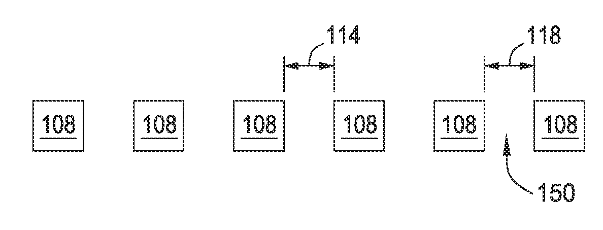
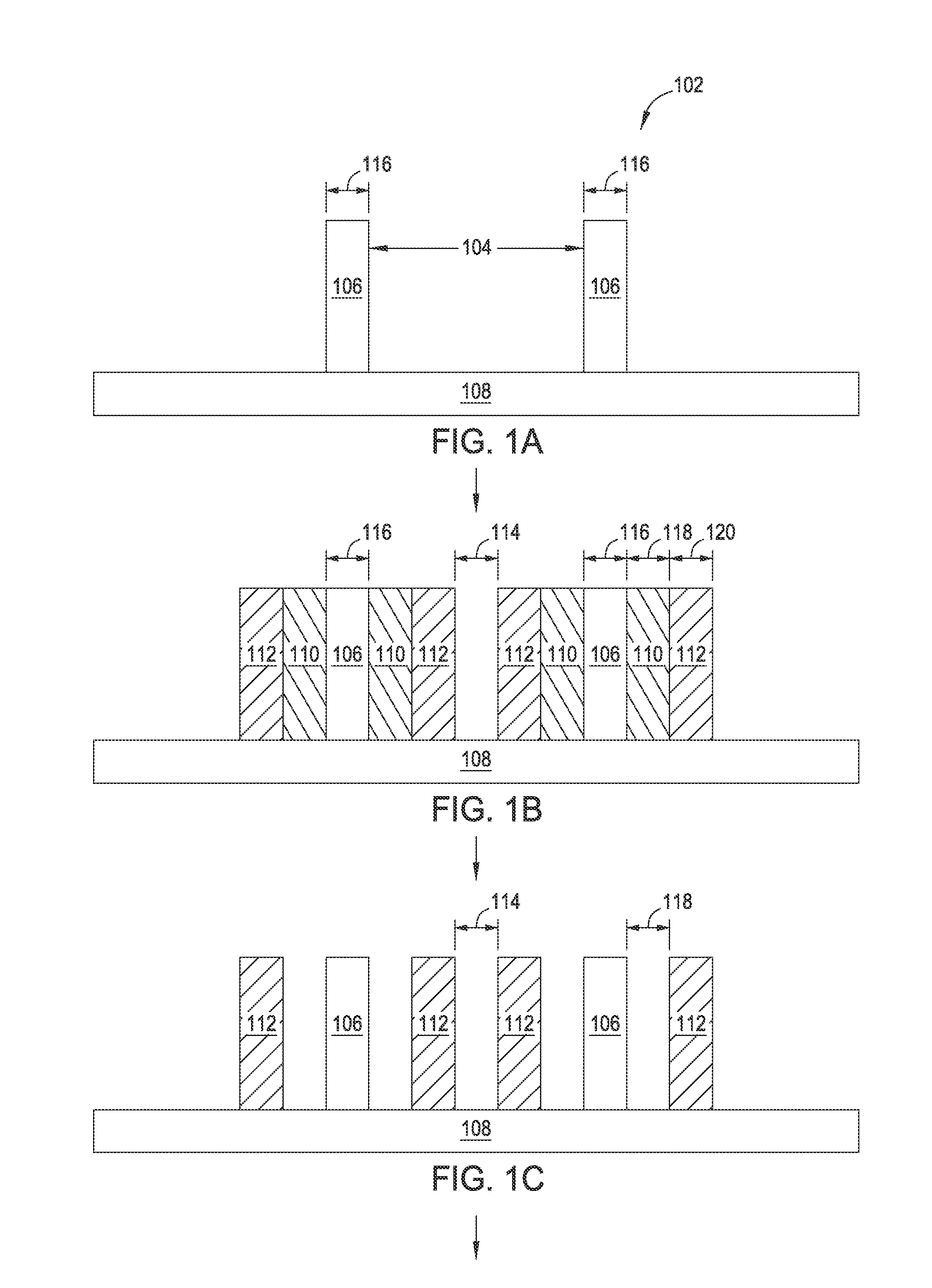
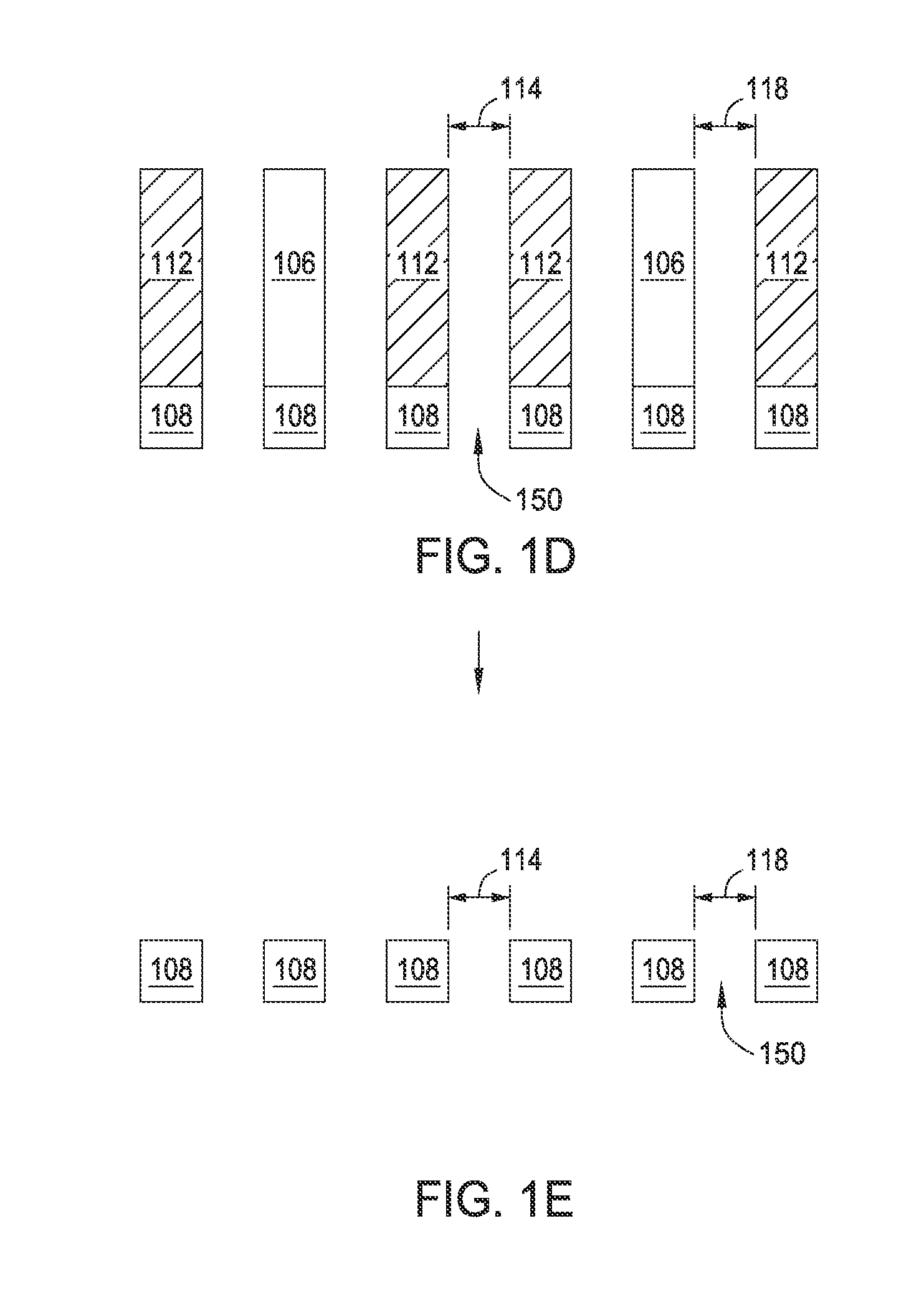
[0019]Methods for manufacturing nanostructures with desired small dimensions, less than 14 nanometers or beyond, are provided. The methods utilize self-aligned multiple spacer patterning (SAMSP) process to transfer features with small dimensions to a mask layer that may be used in an etching process to further transfer features into a material layer disposed underneath the mask layer. The self-aligned multiple spacer patterning (SAMSP) utilizes minimum lithographic exposure process, but rather multiple deposition / etching process to incrementally reduce feature sizes formed in the mask layer along the manufacturing process.

[0020]Referring first to FIG. 4, FIG. 4 is a flow diagram of one example of a method 400 for manufacturing a nanostructure in a mask layer that may be later utilized to serve as an etching mask layer to further transfer features into a material layer disposed underneath the mask layer. FIGS. 1A-1E are cross-sectional views of a portion of a base layer 108 with mult...


PUM

PropertyMeasurementUnit
widthaaaaaaaaaa
widthaaaaaaaaaa
widthaaaaaaaaaa

Abstract

The present disclosure provides forming nanostructures with precision dimension control and minimum lithographic related errors for features with dimension under 14 nanometers and beyond. A self-aligned multiple spacer patterning (SAMSP) process is provided herein and the process utilizes minimum lithographic exposure process, but rather multiple deposition/etching process to incrementally reduce feature sizes formed in the mask along the manufacturing process, until a desired extreme small dimension nanostructures are formed in a mask layer.

Description

CROSS-REFERENCE TO RELATED APPLICATIONS[0001]This application claims benefit of U.S. Provisional Application Ser. No. 62 / 015,227 filed Jun. 20, 2014 (Attorney Docket No. APPM / 22120L), which is incorporated by reference in its entirety.BACKGROUND[0002]1. Field[0003]Examples of the present disclosure generally relate to forming nanostructures in a film layer. Particularly, embodiments of the present disclosure provide methods for forming nanostructures with precision dimension control and minimum lithographic related errors[0004]2. Description of the Related Art[0005]In the manufacture of integrated circuits (IC), or chips, patterns representing different layers of the chip are created by a chip designer. A series of reusable masks, or photomasks, are created from these patterns in order to transfer the design of each chip layer onto a semiconductor substrate during the manufacturing process. Mask pattern generation systems use precision lasers or electron beams to image the design of...

Claims


Application Information

Patent Timeline
Patent Type & Authority Applications(United States)
IPC IPC(8): H01L21/033H01L21/768H01L21/311H01L23/528
CPCH01L21/0332H01L23/528H01L21/0337H01L21/31116H01L21/76816H01L21/31144H01L21/76802
Inventor ZHANG, YINGMITRA, UDAYGOPALRAJA, PRABURAMNEMANI, SRINIVAS D.CHUNG, HUA
Owner APPLIED MATERIALS INC
Why Eureka
Try Eureka