This helps you quickly interpret patents by identifying the three key elements:
Problems solved by technology
Method used
Benefits of technology
[0016]According to the present invention, unnecessary parasitic capacitance can be prevented from being
Problems solved by technology
Such semiconductor integrated circuits are low-voltage drive circuits composed of micro wiring patterns formed on semiconductor substrates, and thus generally fragile against electrostatic discharge such as surge.
When an ESD protection device is provided in a high-frequency circuit, there is the problem of being affected by parasitic capacitance of a diode.
More specifically, the insertion of the ESD device into the signal line shifts impedance under the influence of the parasitic capacitance of the diode, and as a result, loss of signal may be caused.
For this reason
Method used
Image
Click on the blue label to locate the original text in one second.
Reading with bidirectional positioning of images and text.
Examples
Embodiment Construction
[0034]Hereinafter, the semiconductor device according to the present invention will be described with reference to ESD protection devices as examples.
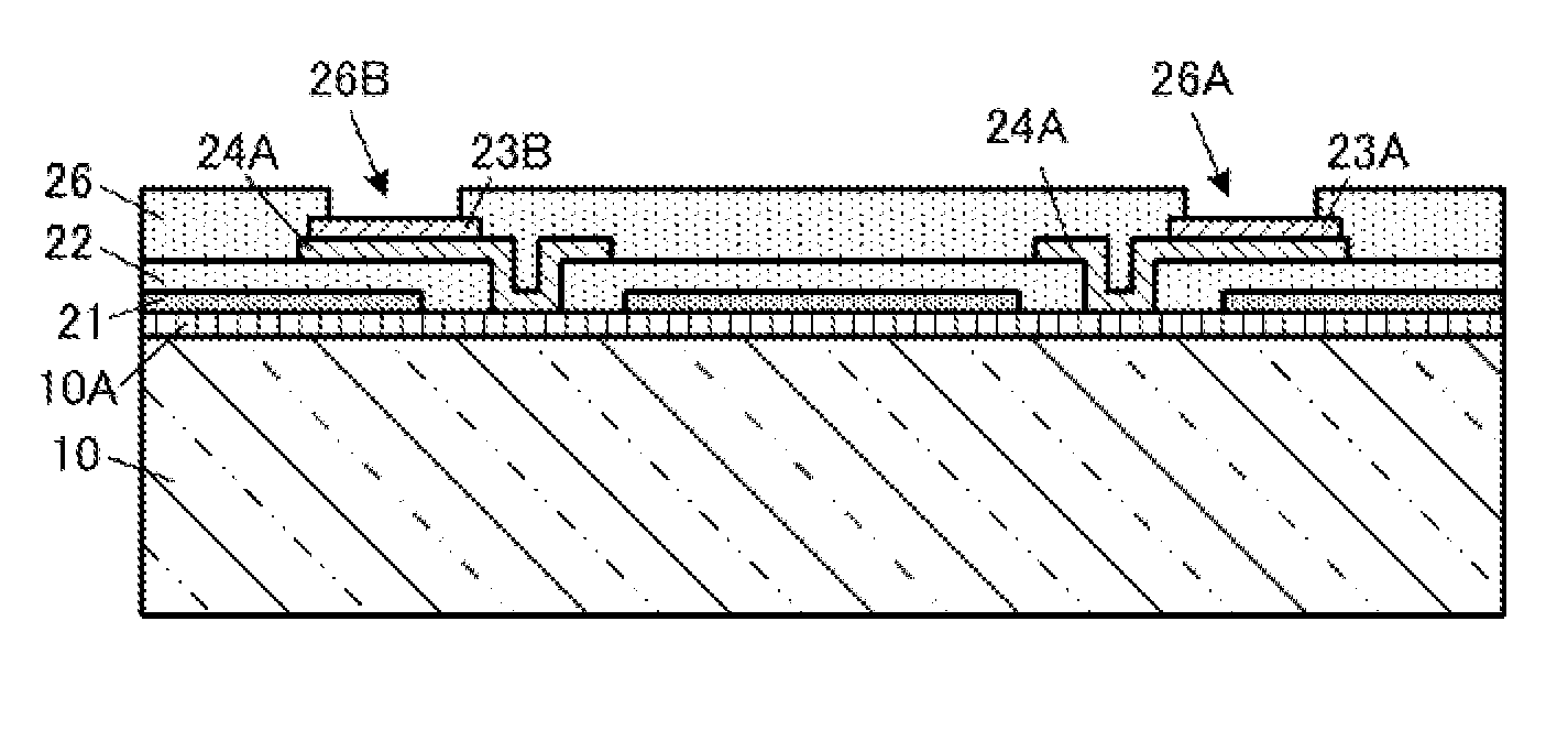
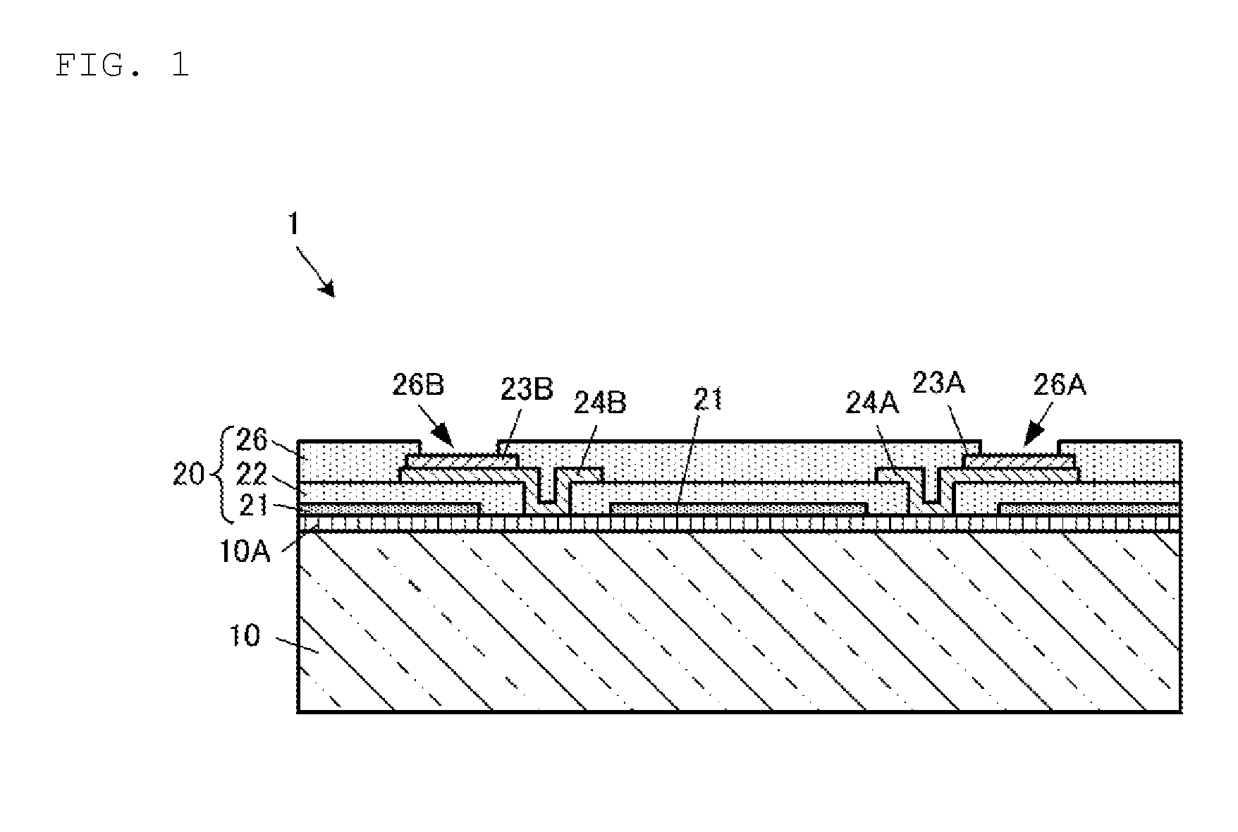
[0035]FIG. 1 is a front cross-sectional view of an ESD protection device 1 according to the present embodiment. FIG. 2 is a plan view of respective layers of the ESD protection device 1. The ESD protection device 1 is a CSP (Chip Size Package) type device, where a rewiring layer 20 including multiple resin layers, etc. is formed on a Si substrate 10 configured to have an ESD protection circuit 10A including a diode and a zener diode. While the Si substrate 10 corresponds to a semiconductor substrate according to the present invention, the semiconductor substrate according to the present invention is not limited to any Si substrate, but may be a GaAs substrate or the like.
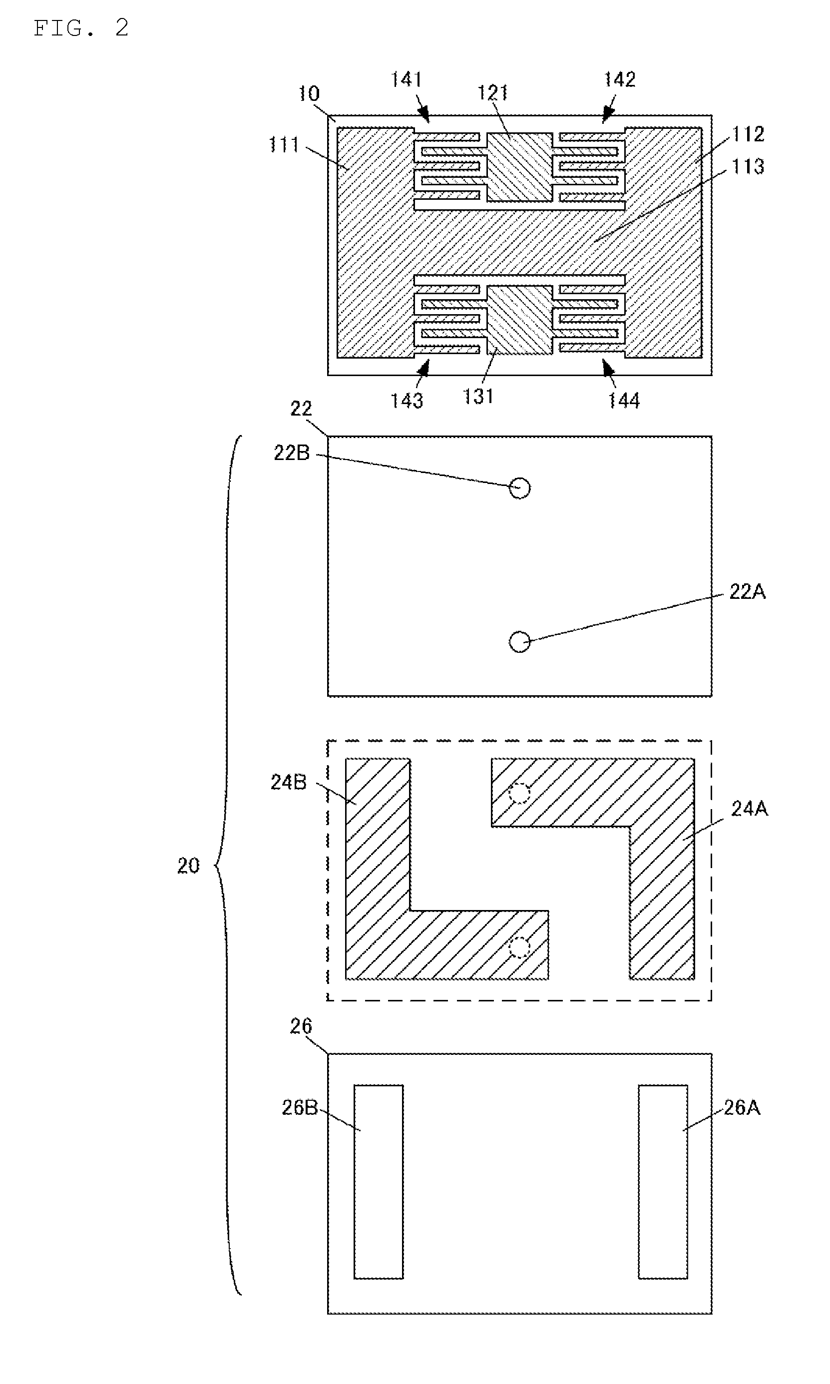
[0036]FIG. 3 is a diagram illustrating the ESD protection circuit 10A formed on the Si substrate 10. FIG. 4 is a diagram illustrating a structure example of the ESD pr...
PUM
Abstract
An ESD protection device includes a Si substrate and a rewiring layer. The rewiring layer includes Ti/Cu/Ti electrodes are electrically connected through contact holes to an ESD protection circuit with Al electrodes films, which is formed at the surface of the Si substrate. The Al electrode film is electrically connected to the Ti/Cu/Ti electrode, whereas the Al electrode film is electrically connected to the Ti/Cu/Ti electrode. A diode forming region is formed between Al electrode films, whereas a diode forming region is formed between Al electrode films. The Ti/Cu/Ti electrode has no overlap with the diode forming region, whereas the Ti/Cu/Ti electrode has no overlap with the diode forming region. Thus, a semiconductor device is provided which is able to reduce the generation of parasitic capacitance, and able to be applied up to a higher frequency band.
Description
CROSS REFERENCE TO RELATED APPLICATIONS[0001]The present application is a continuation of PCT / JP2014 / 054407 filed Feb. 25, 2014, which claims priority to JP Application No. 2013-126659, filed Jun. 17, 2013, JP Application No. 2013-115675, filed May 31, 2013, JP Application No. 2013-097494, filed May 7, 2013, JP Application No. 2013-079960, filed Apr. 5, 2013, JP Application No. 2013-079978, filed Apr. 5, 2013, and JP Application No. 2013-039379, filed Feb. 28, 2013, the entire contents of each of which are incorporated herein by reference.FIELD OF THE INVENTION[0002]The present invention relates to a semiconductor device including a rewiring layer on a semiconductor substrate with a functional element formed.BACKGROUND OF THE INVENTION[0003]An ESD (Electro-Static-Discharge) protection device as a type of semiconductor devices. The ESD protection device protects semiconductor ICs, etc. from static electricity, etc. Various electronic devices including mobile communication terminals, ...
Claims
Application Information
Patent Timeline
Application Date:The date an application was filed.
Publication Date:The date a patent or application was officially published.
First Publication Date:The earliest publication date of a patent with the same application number.
Issue Date:Publication date of the patent grant document.
PCT Entry Date:The Entry date of PCT National Phase.
Estimated Expiry Date:The statutory expiry date of a patent right according to the Patent Law, and it is the longest term of protection that the patent right can achieve without the termination of the patent right due to other reasons(Term extension factor has been taken into account ).
Invalid Date:Actual expiry date is based on effective date or publication date of legal transaction data of invalid patent.