Electorically conductive film

Active Publication Date: 2015-12-24
PANASONIC INTELLECTUAL PROPERTY MANAGEMENT CO LTD
View PDF16 Cites 16 Cited by
  • Summary
  • Abstract
  • Description
  • Claims
  • Application Information

AI Technical Summary

Problems solved by technology

However, ITO exhibits crystalline film characteristics, and therefore breaks easily.
In addition, depletion of resources is a problem with indium used in ITO.
In this type of method, however, it is necessary to use a layer separation mechanism,

Method used


Image

  • Electorically conductive film
  • Electorically conductive film
  • Electorically conductive film

Examples


examples

[0106]First, the various materials used in the present working examples are as follows.

[0107](Thermosetting Resin)[0108]Polyrotaxane (“A1000” manufactured by Advanced Softmaterials, Inc., containing PEG as the axial molecule, alpha-cyclodextrin as the cyclic molecule, and OH groups as reactive groups)[0109]Epoxy resin (“JER1003” manufactured by Mitsubishi Chemical Corp., 7 to 8 methyl groups, 2 functional groups, molecular weight 1300)[0110]Epoxy resin (“EXA-4816” manufactured by DIC Corporation, molecular weight 824, many methyl groups, 2 functional groups)[0111]Epoxy resin “YP50” manufactured by Nippon Steel & Sumikin Chemical Co., Ltd., molecular weight 60,000 to 80,000, many methyl groups, 2 functional groups)[0112]Ethylene oxide adduct type hydroxyphenylfluorene type epoxy resin (“EG-280” manufactured by Osaka Gas Chemicals Co., Ltd.)[0113]Propylene oxide adduct type bisphenol A type epoxy resin (“EP4003S” manufactured by Adeka Corporation)

[0114](Curing Agents)[0115]Polyfunctio...

examples 1 to 9

and Comparative Examples 1 to 3, 5, 7, 9 and 11

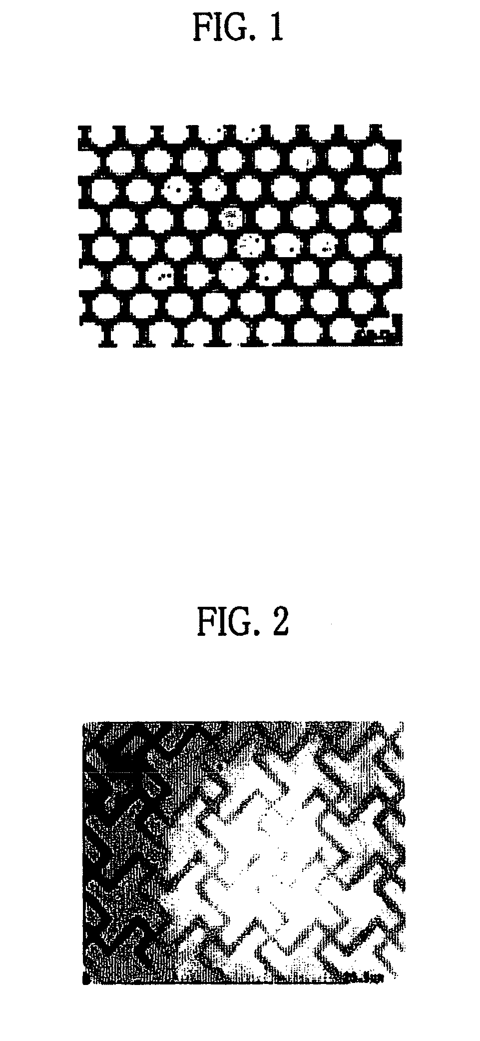
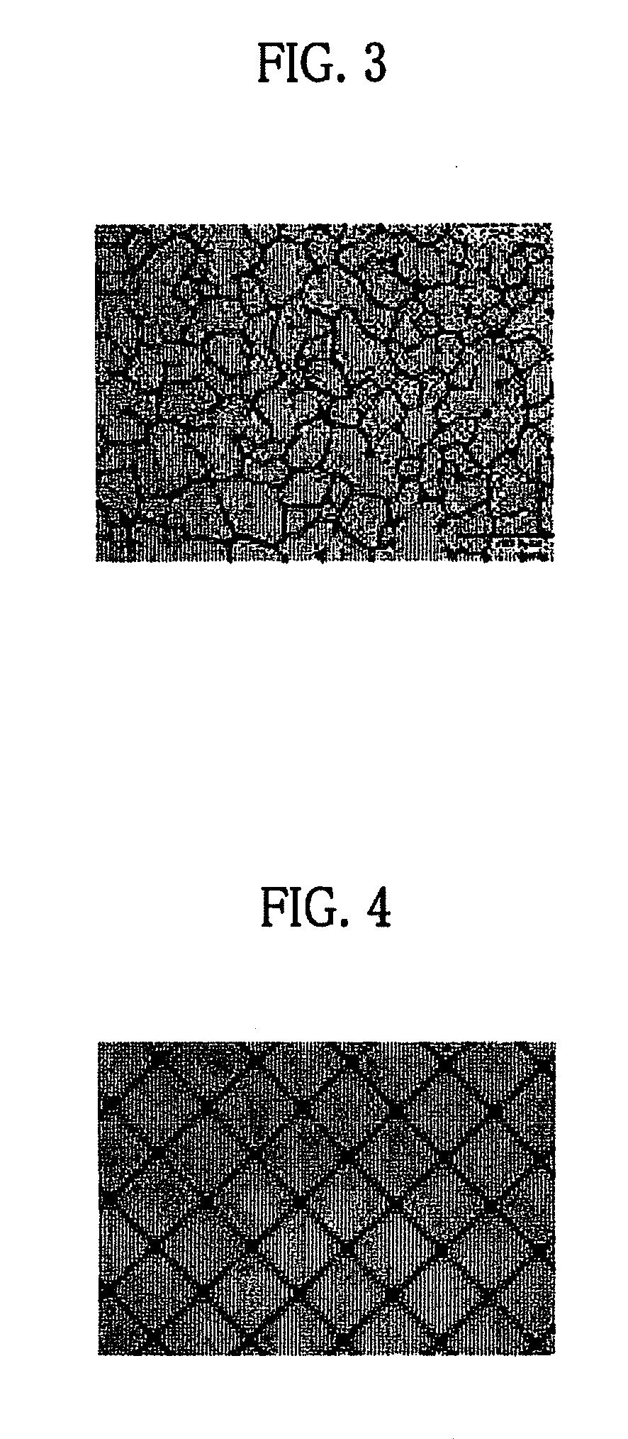
[0124]Mesh-like pattern resist layers were formed by laminating a dry film resist on the resin substrates or films shown in Tables 2 and 3, exposing the resist to light using a mask having a dotted mesh-like pattern, a zigzag mesh-like pattern or a random mesh-like pattern, and then developing. Resin films having mesh-like patterned metal layers were then obtained by vapor depositing the resin films having mesh-like patterned resist layers by a magnetron sputtering method so that the film thickness was 10 nm in the case of gold (Au), 10 nm in the case of silver (Ag) and 100 nm in the case of ITO, and then detaching the resist by means of an aqueous solution of caustic soda.

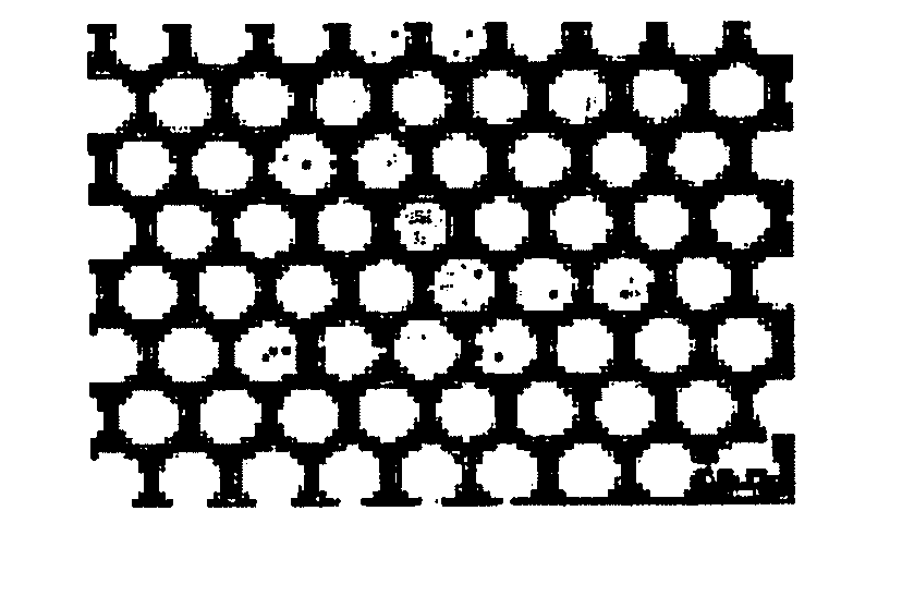
[0125]The metal coverage rate (metal covered area) of the dotted mesh-like pattern was 50% (opening ratio: 50%) and the minimum line width was 30 micrometer (see FIG. 1), the metal coverage rate of the zigzag mesh-like pattern was 30% (opening ratio: 70%) and the mini...

example 10

[0126]A mesh-like pattern resist layer was formed by laminating a dry film resist on a PET film, exposing the resist to light using a mask having a random mesh-like pattern, and then developing. A PET film having a mesh-like patterned metal layer was then obtained by vapor depositing the PET film having a mesh-like patterned resist layer by a magnetron sputtering method so that the Ag film thickness was 10 nm, and then detaching the resist by means of an aqueous solution of caustic soda. The PET film having a mesh-like patterned metal layer was immersed in an aqueous solution of an electrodeposition resist (Elecoat PI, manufactured by Shimizu Co., Ltd.), thereby electrodepositing a resist resin on the metal layer. A resin film having a thickness of 50 micrometer was obtained on the PET film having an electrodeposited mesh-like patterned metal layer by coating the resin composition for the resin substrate 5 on the surface of the PET film having an electrodedeposited mesh-like pattern...


PUM

PropertyMeasurementUnit
Temperatureaaaaaaaaaa
Fractionaaaaaaaaaa
Fractionaaaaaaaaaa

Abstract

The present invention relates to an electrically conductive film characterized by being able to undergo elastic deformation, having little residual strain rate and exhibiting stress relaxation properties. More specifically, the present invention relates to an electrically conductive film wherein the stress relaxation rate (R) and the residual strain rate a, as measured in a prescribed extension-restoration test, are as follows: 20%≦R≦95% and 0%≦α≦3%.

Description

TECHNICAL FIELD[0001]The present invention relates to an electrically conductive film having high tensile stress relaxation properties and excellent recoverability following extension.BACKGROUND ART[0002]Transparent electrodes, which are electrically conductive materials, exhibit excellent light transmission properties, electrical conductivity, and the like, and are therefore used in a wide variety of fields, such as display devices equipped with touch panels. As we have moved towards an ambient information society in recent years, there has been a desire to develop wearable electronic devices which are not restricted by real space and which can be worn on the body.[0003]Indium tin oxide (hereinafter abbreviated in ITO) can be given as an example of an electrically conductive material used in the past in touch panel displays. However, ITO exhibits crystalline film characteristics, and therefore breaks easily. Therefore, in cases where a PET film, for example, is used as a flexible s...

Claims


Application Information

Patent Timeline
IPC IPC(8): H05K1/02G06F3/041H05K1/03H01B1/02H01L31/0224
CPCC09D105/16B32B2307/202B32B2260/046C08J5/18C08K7/02C08L101/00Y10T428/24917H05K2201/0108H05K1/0333H05K1/0326H05K1/0296H05K2201/012H05K1/0271H01L31/022491H01B1/02G06F3/041H05K1/0274B32B15/092B32B15/08Y10T428/24331B32B2363/00B32B2307/412C09D163/00B32B2307/50B32B3/12B32B3/266C08J2400/21C08J7/047C08J2300/21C08J2367/02C08J2463/00H05K1/0213H01L31/022466H01B1/24B32B2262/14B32B2262/106B32B2262/103H05K2201/0326B32B2260/021B32B5/02H05K2201/0323H05K1/0366H05K1/028C08L63/00C08J7/0427
Inventor SAWADA, TOMOAKIYOSHIOKA, SHINGOABE, TAKATOSHI
Owner PANASONIC INTELLECTUAL PROPERTY MANAGEMENT CO LTD
Why Eureka
Try Eureka