Silicon Dry Etching Method

a technology of silicon and etching method, which is applied in the direction of basic electric elements, semiconductor/solid-state device manufacturing, electrical equipment, etc., can solve the problems of large electrical damage to samples, no reports that actually use iodine heptafluoride for etching applications, and increase the cost of equipment, so as to avoid the effect of equipment load and good uniformity of in-plane etching

Active Publication Date: 2016-01-07
CENT GLASS CO LTD
View PDF2 Cites 6 Cited by
  • Summary
  • Abstract
  • Description
  • Claims
  • Application Information

AI Technical Summary

Benefits of technology

[0027]As mentioned above, the present invention utilizes the iodine heptafluoride-containing etching gas and enables adiabatic expansion of the etching gas under milder pressure conditions than conventional method. It is therefore possible in the present invention to etch the processing target silicon layer with good uniformity of in-plane etching amount distribution even under mile pressure conditions with no need to set the supply pressure of the etching gas to a high level and with no fear of equipment load and increase in equipment cost by nozzle modification etc.

Problems solved by technology

In the conventional plasma etching methods, however, there occurs large electrical damage to samples by plasma.
Concerns are thus rising that, in the case of plasma etching silicon on complicated shaped semiconductor elements, etching-resistant parts such as dielectric parts of the semiconductor elements may also become damaged.
There are however no reports that actually use iodine heptafluoride for etching applications and discuss the conditions of etching with iodine heptafluoride.

Method used


Image

  • Silicon Dry Etching Method
  • Silicon Dry Etching Method
  • Silicon Dry Etching Method

Examples


example 1-1

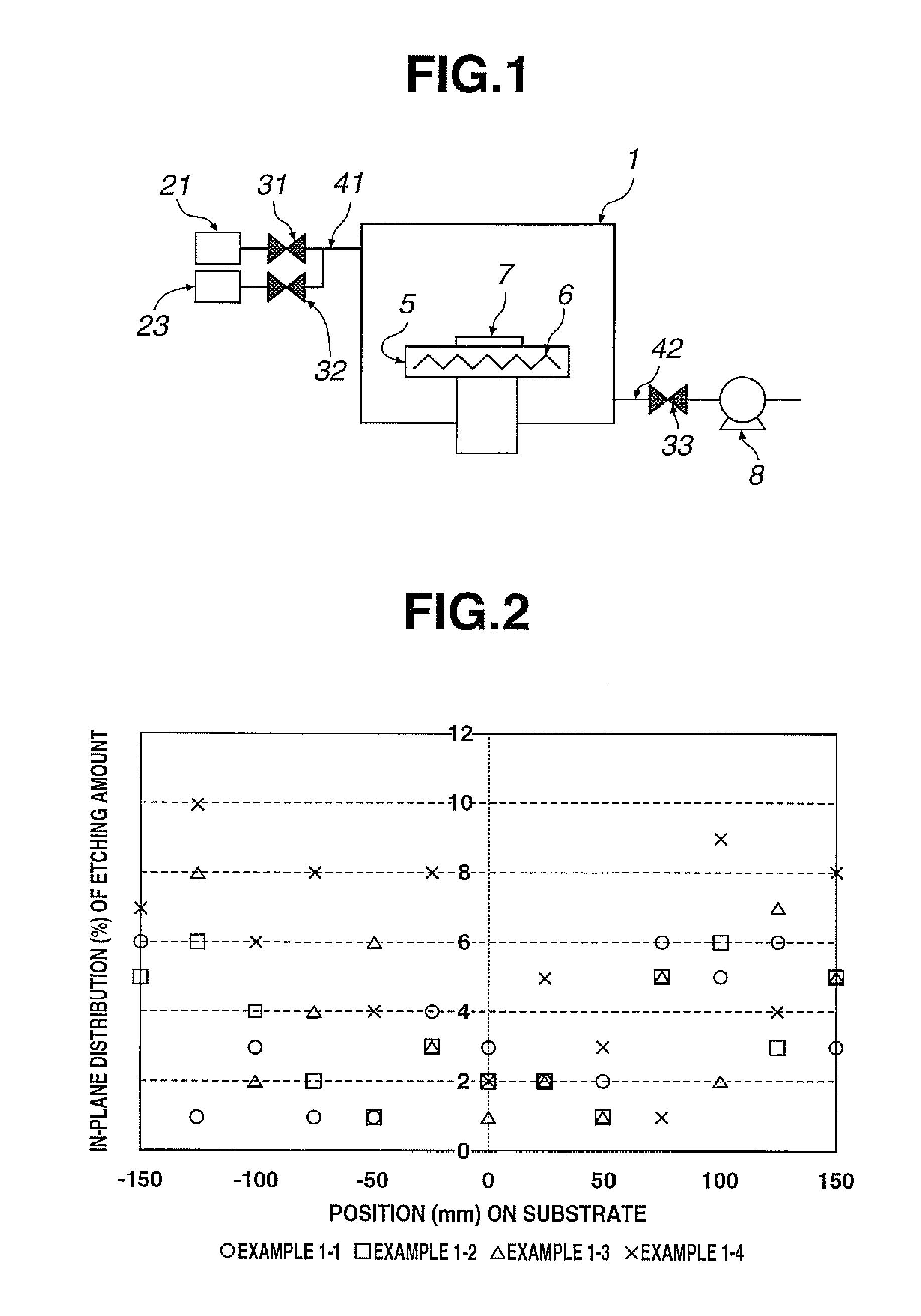
[0067]The sample was subjected to etching test with the use of the etching gas containing substantially no component other than iodine heptafluoride (IF7, volume fraction: 100%, no diluent gas). As to the etching conditions, the supply gas of the etching gas was set to 100 Pa; the etching processing pressure inside the chamber was set to 1 kPa; the total flow rate of the etching gas was set to 100 sccm; and the temperature of the silicon substrate was set to 30° C. As a result, the in-plane etching amount distribution of the sample after the etching test was 1 to 6%. The sample thus had good in-plane etching uniformity. Further, the etching rate was at a favorable level of 12 μm / min. In Example 1-1, the ratio Ps / Pn between the supply pressure (Ps) of the etching gas and the internal pressure (Pn) of the processing room was 66.

example 1-2

[0068]The etching test was performed under the same conditions as those in Example 1-1 except that the etching gas contained 80 vol % of iodine heptafluoride (and 20 vol % of Ar gas). As a result, the in-plane etching amount distribution of the sample after the etching test was 1 to 6% as in the case of Example 1-1. The sample thus had good in-plane etching uniformity. The etching rate was at a favorable level of 11 μm / min.

example 1-3

[0069]The etching test was performed under the same conditions as those in Example 1-1 except that the etching gas contained 50 vol % of iodine heptafluoride (and 50 vol % of Ar gas). As a result, the in-plane etching amount distribution of the sample after the etching test was 1 to 8%. The sample had generally satisfactory in-plane etching uniformity although it was slightly inferior to those in Examples 1-1 and 1-2. The etching rate was at a relatively favorable level of 5 μm / min although it was lower than that in Example 1-1.


PUM


Abstract

A dry etching method according to the present invention is for etching a silicon layer as a processing target in a processing room, characterized by supplying an iodine heptafluoride-containing etching gas from a gas supply source at a supply pressure of 66 kPa to 0.5 MPa, evacuating the processing room to an internal pressure lower than the supply pressure of the etching gas and, while maintaining the etching gas at the supply pressure, introducing the etching gas into the evacuated processing room so as to etch the silicon layer by the etching gas. It is possible by this dry etching method to etch the silicon upon adiabatic expansion of the etching gas under mild pressure conditions, with no fear of equipment load and equipment cost increase, and achieve good uniformity of in-plane etching amount distribution.

Description

FIELD OF THE INVENTION[0001]The present invention relates to a method for dry etching of silicon with the use of iodine heptafluoride.BACKGROUND ART[0002]Silicon and its compounds are important and inevitable materials in the fields of semiconductors. These materials have a wide range of applications including, for example, silicon oxide films as gate insulators for semiconductor devices, amorphous silicon films and silicon nitride films as thin-film transistors, polysilicon films for three-dimensional structural elements such as MEMS, silicon carbide (SiC) films for low-power-consumption transistors and the like. Attention is particularly given to silicon semiconductor devices under the circumstance that the high-density integration of semiconductor elements, as typified by transistors for DRAM and flash memories, has been proceeding year after year.[0003]During semiconductor manufacturing, silicon and its compounds are commonly processed into predetermined shapes or removed by pre...

Claims


Application Information

Patent Timeline
Patent Type & Authority Applications(United States)
IPC IPC(8): H01L21/3065
CPCH01L21/3065
Inventor KIKUCHI, AKIOUMORI, ISAMUWATARI, MASANORI
Owner CENT GLASS CO LTD
Why Eureka
Try Eureka