Secondary battery and electronic device including the same

Active Publication Date: 2016-01-14
SEMICON ENERGY LAB CO LTD
View PDF0 Cites 33 Cited by
  • Summary
  • Abstract
  • Description
  • Claims
  • Application Information

AI Technical Summary

Benefits of technology

[0033]When an electrode is bent by bending the secondary battery, generation of a crack in the electrode due to the stretching of an end portion of the electrode is prevented because part of the electrode or part of the active material layer is cut. As

Problems solved by technology

A metal can that is used as an exterior body has a problem of increasing the weight of a secondary battery.
Moreover, it is difficult to manufac

Method used


Image

  • Secondary battery and electronic device including the same
  • Secondary battery and electronic device including the same
  • Secondary battery and electronic device including the same

Examples


embodiment 1

[0052]In this embodiment, an electrode for a secondary battery and a method for manufacturing a secondary battery according to one embodiment of the present invention will be described with reference to FIGS. 1A to 1D, FIGS. 2A to 2D, FIGS. 3A to 3D, FIGS. 4A to 4E, and FIGS. 5A to 5F.

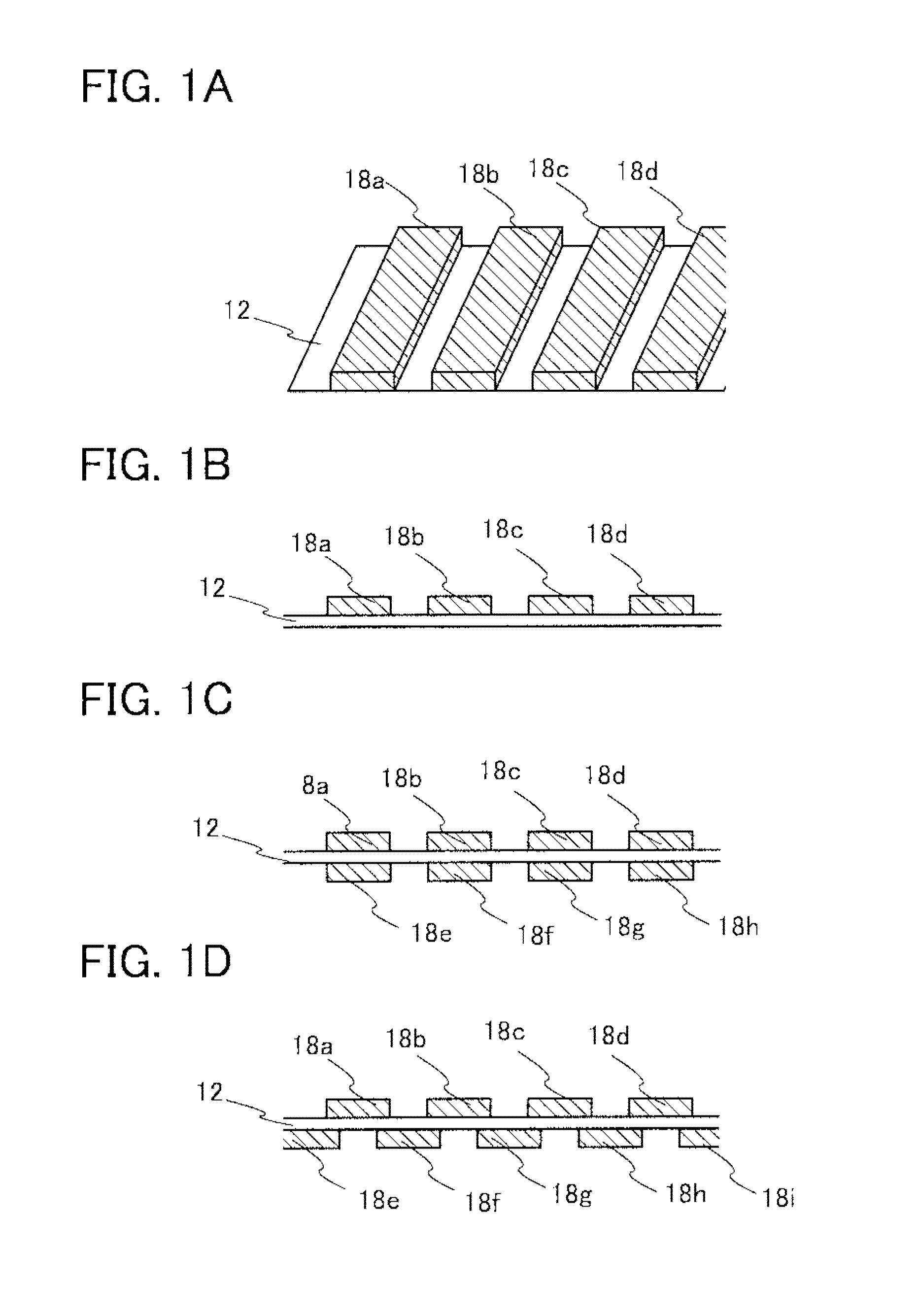
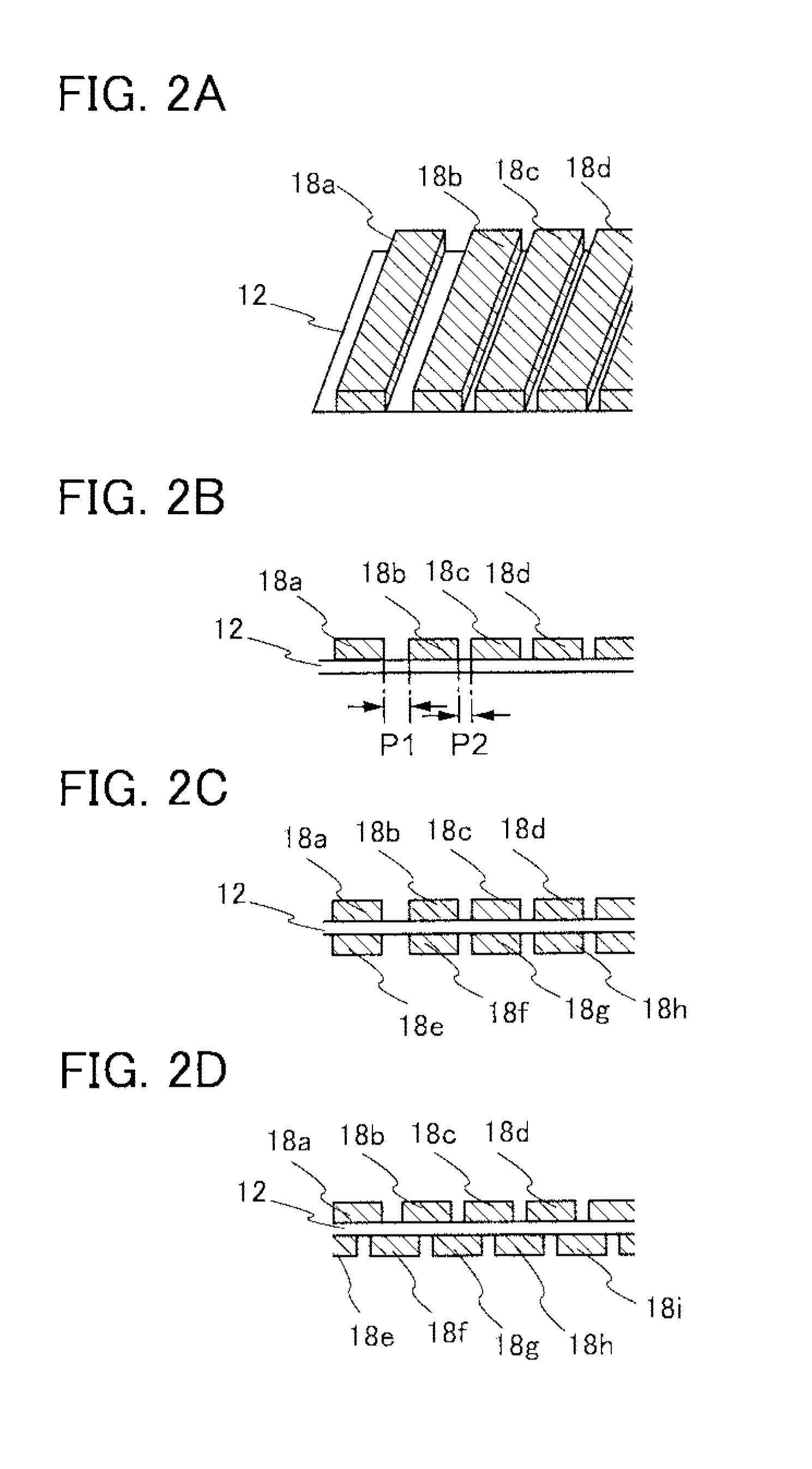
[0053]FIG. 1A is a perspective view illustrating a plurality of positive electrode active material layers formed on a positive electrode current collector 12, and FIG. 1B is a cross-sectional view thereof. The plurality of positive electrode active material layers are formed in contact with one surface of the positive electrode current collector 12. In other words, the plurality of positive electrode active material layers are formed in a plurality of divided regions in contact with one surface of the positive electrode current collector 12.

[0054]The manufacturing method is as follows: after slurry is applied and dried, a positive electrode active material layer is partly removed by laser light irradia...

embodiment 2

[0103]In this embodiment, an example of manufacturing a secondary battery using a current collector including a meandering portion will be described below.

[0104]First, a positive electrode active material layer is formed on one or both surfaces of a band-like metal foil.

[0105]Next, laser light irradiation is performed to selectively remove the positive electrode active material layer. The positive electrode active material layer over two areas, which are a region having a small width that is connected to an electrode lead in a later step and an area having a small width in a meandering portion, is removed. Then, laser processing is performed to selectively remove both the positive electrode active material layer and the metal foil. Here, the laser irradiation is performed so that the contour of the current collector including the meandering portion is irradiated; thus, the shape of the current collector is formed. At this stage, the state illustrated in FIG. 6A can be obtained. As i...

embodiment 3

[0130]In this embodiment, examples of electronic devices incorporating the lithium-ion secondary battery described in Embodiment 1 or 2 will be described.

[0131]In the secondary battery described in Embodiment 1 or 2, the active material layer is partly removed; therefore, the stress applied to the secondary battery when the secondary battery is bent can be relieved. This secondary battery can be bonded to a support structure body with a curved surface and can change its form reflecting the curved surface of a region of the support structure body that has a large radius of curvature.

[0132]Examples of electronic devices each using a flexible power storage device are as follows: display devices (also referred to as televisions or television receivers) such as head-mounted displays and goggle type displays, desktop personal computers, notebook personal computers, monitors for computers or the like, cameras such as digital cameras or digital video cameras, digital photo frames, electroni...


PUM


Abstract

An electronic device having a novel structure, specifically, an electronic device having a novel structure that can be changed into various appearances is provided. Specifically, after an active material layer is formed on one or both surfaces of a current collector, the active material layer in a bent region is partly removed. The removed region of the active material layer can be in a linear shape, a dot shape, or a matrix shape, for example. After the active material layer is formed on one or both surfaces of the current collector, laser processing for removing part of the active material layer in an irradiation region is performed using laser light or the like. On the region where the surface of the current collector is exposed, the active material layer is not provided, and this region is a region that does not function as a battery. Owing to this region, a secondary battery with a wide movable region can be achieved.

Description

BACKGROUND OF THE INVENTION[0001]1. Field of the Invention[0002]One embodiment of the present invention relates to an object, a method, or a manufacturing method. The present invention relates to a process, a machine, manufacture, or a composition of matter. One embodiment of the present invention relates to a method for manufacturing a semiconductor device, a display device, a light-emitting device, a power storage device, a lighting device, or an electronic device. In particular, one embodiment of the present invention relates to an electronic device and its operating system.[0003]Note that electronic devices in this specification generally mean devices including secondary batteries, and electro-optical devices including secondary batteries, information terminal devices including secondary batteries, and the like are all electronic devices.[0004]2. Description of the Related Art[0005]Electronic devices carried around by users and electronic devices worn by users have been actively...

Claims


Application Information

Patent Timeline
IPC IPC(8): H01M2/02H01M4/13H01M4/02H01M4/66H01M4/70H01M10/0525H01M10/0566H01M10/0585
CPCH01M4/13H01M2/02H01M4/661H01M10/0525H01M2004/027H01M2220/30H01M2220/20H01M2004/028H01M4/70H01M4/139H01M2004/021H01M10/058H01M4/0435Y02E60/10
Inventor TAJIMA, RYOTAGOTO, YUUGOYONEDA, YUMIKOGOTO, JUNYAMIWA, TAKUYAHIROKI, MASAAKI
Owner SEMICON ENERGY LAB CO LTD
Why Eureka
Try Eureka