Driving device for semiconductor elements, and semiconductor device

Active Publication Date: 2016-01-28
MITSUBISHI ELECTRIC CORP
View PDF2 Cites 21 Cited by
  • Summary
  • Abstract
  • Description
  • Claims
  • Application Information

AI Technical Summary

Benefits of technology

[0019]According to the present invention, the capacitive element is rapidly charged after a timed point at which the voltage across the capacitive element becomes equ

Problems solved by technology

This collector current detection method is thought to be ineffective in accurately detecting the collector curre

Method used


Image

  • Driving device for semiconductor elements, and semiconductor device
  • Driving device for semiconductor elements, and semiconductor device
  • Driving device for semiconductor elements, and semiconductor device

Examples


embodiment 1

(Functions and Advantages of Embodiment 1)

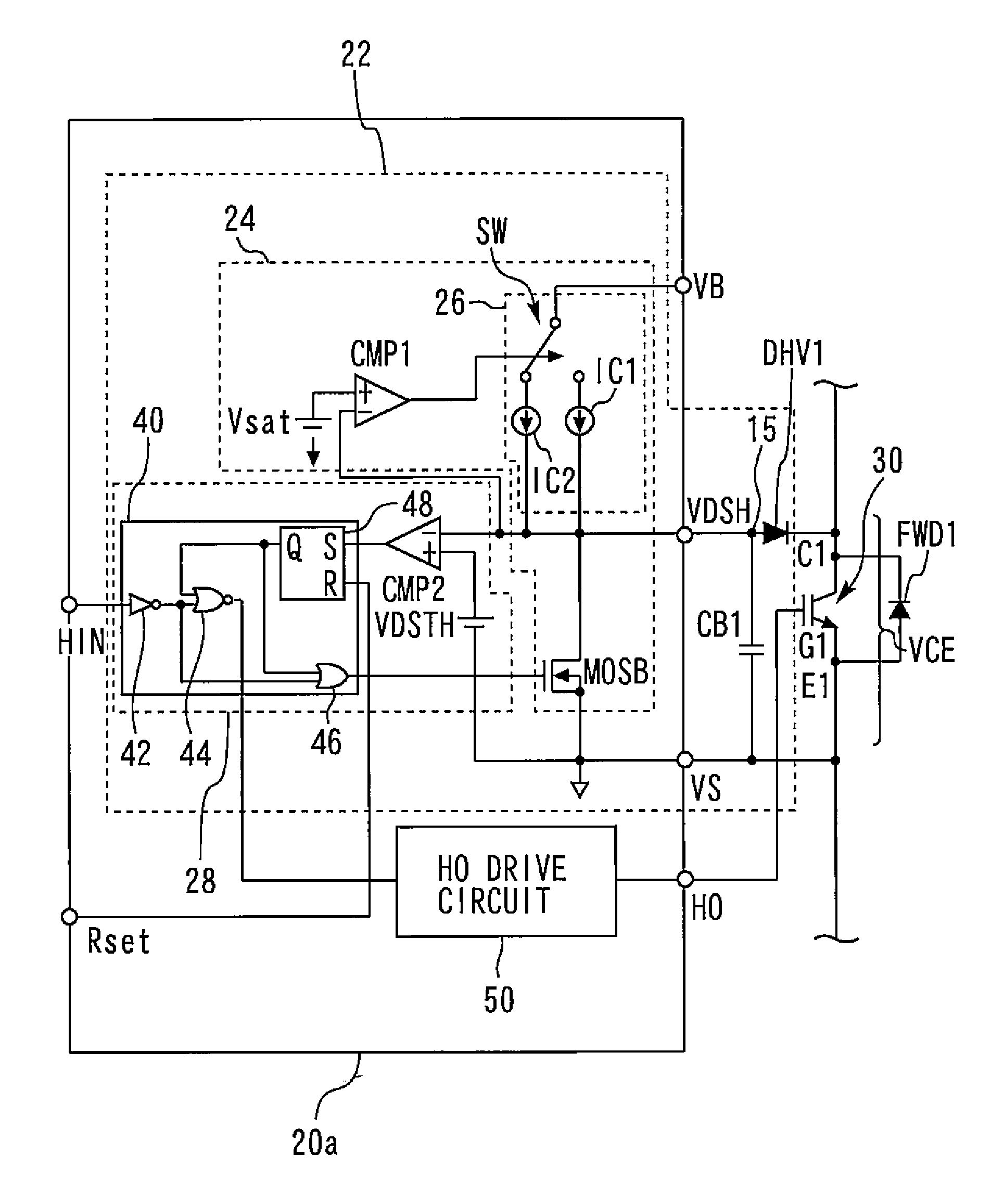
[0145]In the desat detection circuit section 22, the blanking time is set with the blanking capacitive element CB1. The mechanism using the blanking time is such that the detection of a non-saturation voltage is not immediately recognized as the occurrence of a short circuit; if a time period during which a non-saturation voltage is detected in the on-state after turn-on exceeds the blanking time, it is determined that the occurrence of a short circuit is sensed.

[0146]This blanking time setting enables avoidance of erroneous detection of the normal non-saturation voltage state immediately after turn-on. However, this blanking time also has an influence even when a short circuit occurs during the operation in the on-state of the IGBT 30 after the saturation voltage is once reached after turn-on.

[0147]In this respect, in the present embodiment, an increase in the collector-emitter voltage VCE from the saturation voltage (non-saturation) once t...

embodiment 2

[0153]FIG. 8 is a circuit diagram showing the configuration of a driving device for semiconductor elements according to Embodiment 2 of the present invention and components on the periphery of the driving device for semiconductor elements. The driving device for semiconductor elements according to Embodiment 2 is HVIC 220a. The HVIC 220a and the external circuit form a desat detection circuit section 222. The desat detection circuit section 222 has the same configuration as that of the desat detection circuit section 22 according to Embodiment 1 except for the configuration of a charging circuit section 224 (constant current supply section 226 in particular).

[0154]It is assumed that, except for the above-descried points of difference, a semiconductor device according to Embodiment 2 has the same configuration as that of the semiconductor device (inverter device 10) according to Embodiment 1, and that the driving device for semiconductor elements according to Embodiment 2 has the sam...

embodiment 3

[0158]FIG. 10 is a circuit diagram showing the configuration of a driving device for semiconductor elements according to Embodiment 3 of the present invention and components on the periphery of the driving device for semiconductor elements. The driving device for semiconductor elements according to Embodiment 3 is HVIC 320a. The HVIC 320a and the external circuit form a desat detection circuit section 322. The HVIC 320a has the same configuration as that of the HVIC 220a according to Embodiment 2 except for the configuration of a charging circuit section 324. The charging circuit section 324 has the same configuration as that of the charging circuit section 224 except for a hysteretic comparator CMPH substituted for the comparator CMP1.

[0159]It is assumed that, except for the above-descried points of difference, a semiconductor device according to Embodiment 3 has the same configuration as that of the semiconductor device according to Embodiment 2, and that, with the same exceptions...


PUM


Abstract

The device for driving the semiconductor element is provided with a drive circuit section, a charging circuit section and a shutting circuit section. The charging circuit section is electrically connected to an external circuit provided with a diode and a capacitive element. The semiconductor element has a first electrode, a second electrode and a control terminal. The cathode of the diode is connected to the first electrode. One of two terminals of the capacitive element is connected to the cathode of the diode, and the other terminal is connected to the second electrode. The charging circuit section enables the capacitive element to be charged at a higher rate after a timed point at which the voltage on the capacitive element becomes equal to a saturation voltage in a case where the input signal is an on-signal.

Description

TECHNICAL FIELD[0001]The present invention relates to a driving device for semiconductor elements and to a semiconductor device.BACKGROUND ART[0002]Conventionally, a driving device for semiconductor elements capable of coping with the possibility of damage to a semiconductor element caused by an excess current due to a short circuit, as disclosed in Japanese Patent Laid-Open No. 2002-208847 for example, is known. By detecting a collector current in a semiconductor element such as an IGBT, gate shutting for example, which is a protective operation at the time of detection of an excess current, is performed.[0003]Detection of a collector current in a semiconductor element from a collector-emitter voltage VCE detected with a diode is performed. This collector current detection method is thought to be ineffective in accurately detecting the collector current from the VCE detection value in a time period of several microseconds from turn-on to entering a steady state. On the other hand, ...

Claims


Application Information

Patent Timeline
IPC IPC(8): H02H3/08H03K17/082
CPCH03K17/0822H02H3/08H03F1/52H03F3/217
Inventor HABU, YOYAMAMOTO, MASAHIRO
Owner MITSUBISHI ELECTRIC CORP
Why Eureka
Try Eureka