
Memory Processing Core Architecture

a core architecture and memory technology, applied in the field of computer technology, can solve the problems of significant time and energy consumption, inefficient architecture, and the inability to efficiently transfer entire pieces, and achieve the effects of increasing system performance, increasing power efficiency, and efficient offloading whole pieces

Active Publication Date: 2016-02-11
WISCONSIN ALUMNI RES FOUND
View PDF13 Cites 20 Cited by
  • Summary
  • Abstract
  • Description
  • Claims
  • Application Information

AI Technical Summary

Benefits of technology

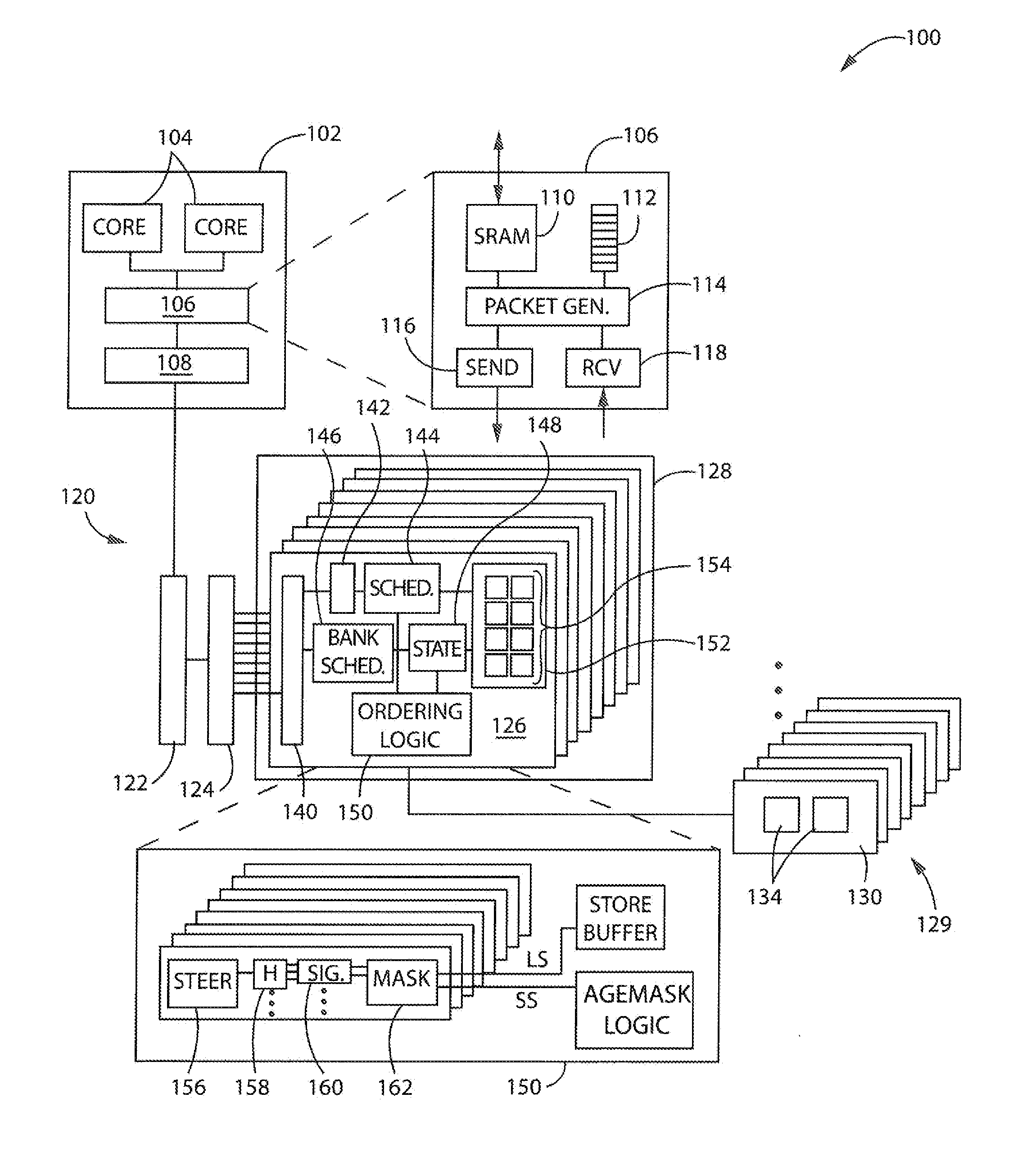
The present invention is about improving the performance of computer systems by using memory processing cores that are tightly coupled with memory layers to create memory vaults. By segmenting application code into discrete parts and storing them in specific memory vaults, a host processor can offload computation to the memory processing core, resulting in faster processing with reduced power consumption. In summary, this invention is about providing optimal processing capability localized to a memory section targeted for a partition of application code at runtime, with maximized efficiency for transferring bits with reduced power consumption.

Problems solved by technology

Such architectures are inefficient to the extent that significant time and energy are consumed to move information between the processor cores and the tiered memory structure.
For example, if a closer memory does not contain the necessary instructions or data required by the processor, depending on the distance between the processor and the memory containing the required information, the computer system could suffer from significantly greater access latencies and power consumed simply by transferring bits between circuits than would otherwise be necessary.

Method used


Image

  • Memory Processing Core Architecture
  • Memory Processing Core Architecture
  • Memory Processing Core Architecture

Examples


Embodiment Construction

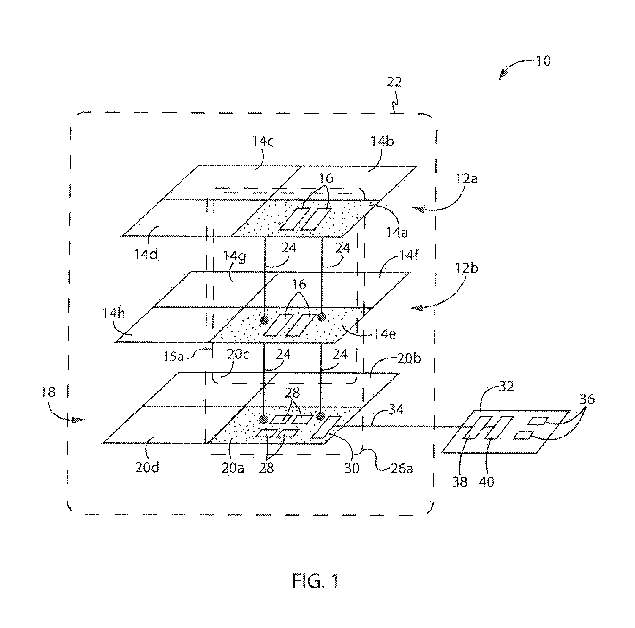
[0027]Referring now to FIG. 1, an embodiment of the present invention will be described in the context of a computer system 10. The computer system 10 could be implemented in a variety of applications, including, for example, a laptop, tablet, smart phone or other mobile computing device, a desktop computer, a server, a network router, switch or hub, and the like.

[0028]In the computer system 10, a plurality of memory layers 12 are “stacked,” or arranged in a three-dimensional (3D) configuration in which layers are physically arranged one over the other, such as by wafer-on-wafer or die-on-wafer processes, with the memory layers 12 physically being coupled together. Each memory layer 12 comprises a separate die or “chip” in which one is fabricated over the other, or stacked adjacently, using conventional monolithic 3D fabrication techniques. In this example, for simplicity, two adjacent memory layers are shown, including an upper memory layer 12a and a lower memory layer 12b.

[0029]T...


PUM


Abstract

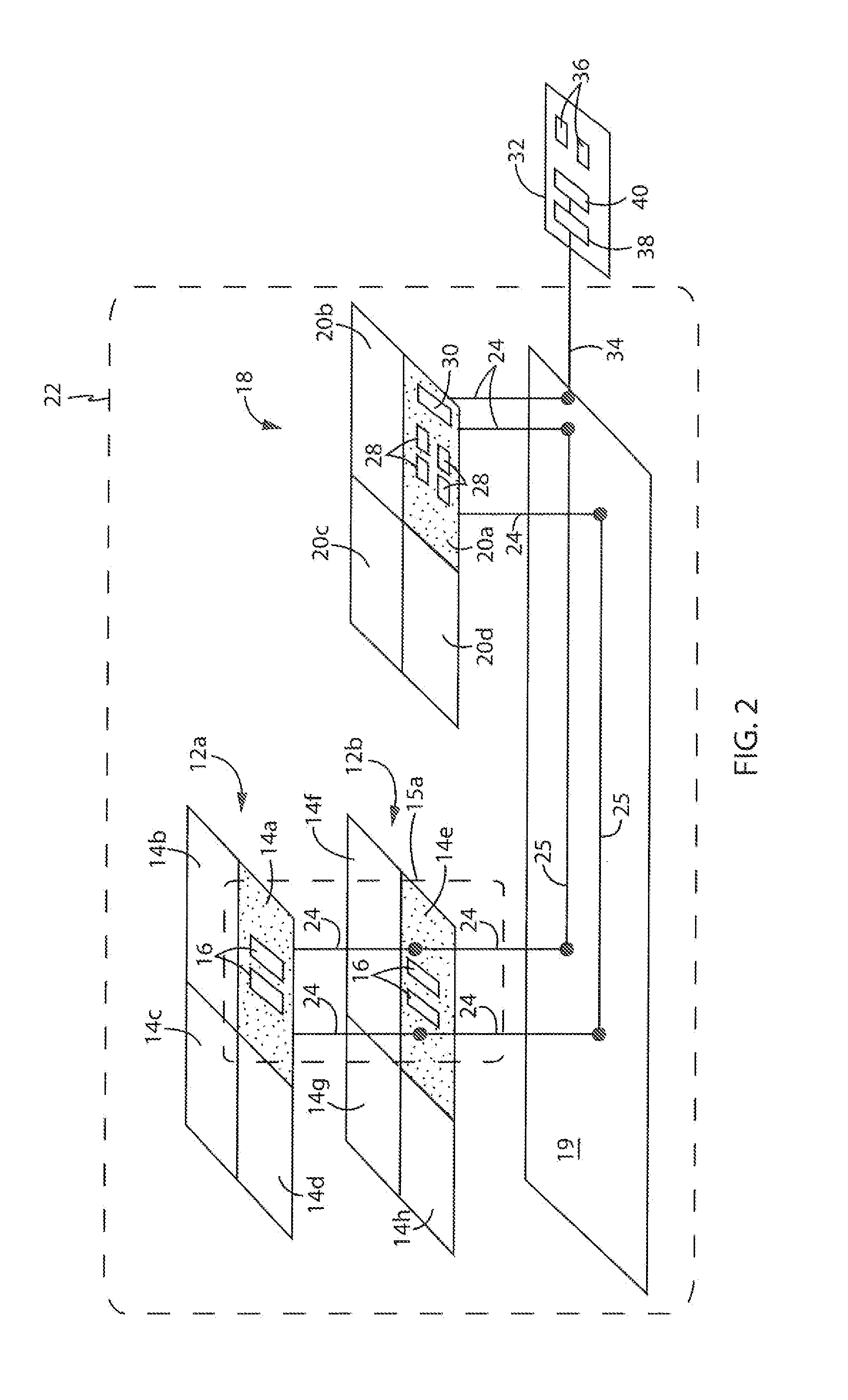
Aspects of the present invention provide a memory system comprising a plurality of stacked memory layers, each memory layer divided into memory sections, wherein each memory section connects to a neighboring memory section in an adjacent memory layer, and a logic layer stacked among the plurality of memory layers, the logic layer divided into logic sections, each logic section including a memory processing core, wherein each logic section connects to a neighboring memory section in an adjacent memory layer to form a memory vault of connected logic and memory sections, and wherein each logic section is configured to communicate directly or indirectly with a host processor. Accordingly, each memory processing core may be configured to respond to a procedure call from the host processor by processing data stored in its respective memory vault and providing a result to the host processor. As a result, increased performance may be provided.

Description

STATEMENT REGARDING FEDERALLY SPONSORED RESEARCH[0001]This invention was made with government support awarded by the National Science Foundation. The government has certain rights in the invention.BACKGROUND OF THE INVENTION[0002]The present invention relates to computer technologies, and more particularly, to memory systems for computers.[0003]Modern computer architectures typically provide one or more multi-core processors connected to a tiered memory structure that includes various levels of caches and a main memory. As a processor executes application code that is part of an instruction stream, the processor must continually retrieve instructions and data from the tiered memory structure for processing. If a faster, proximally closer memory, such as a Level 1 cache, does not contain the necessary instructions or data required by the processor, the processor must typically wait for a slower, more distant memory, such as a Level 2 or 3 cache or a main memory, to provide the inform...

Claims


Application Information

Patent Timeline
Patent Type & Authority Applications(United States)
IPC IPC(8): G06F9/54
CPCG06F9/547G06F15/7821Y02D10/00
Inventor SANKARALINGAM, KARTHIKEYANMENON, JAIKRISHNANDE CARLI, LORENZO
Owner WISCONSIN ALUMNI RES FOUND
Learn More