Laser assisted bonding for semiconductor die interconnections

a technology of interconnection and laser assisted bonding, which is applied in the direction of printed circuit assembling, printed circuit manufacturing, printed circuit aspects, etc., can solve the problems of electrical disconnection between the semiconductor die and the circuit board

Active Publication Date: 2016-02-18
AMKOR TECH SINGAPORE HLDG PTE LTD
View PDF11 Cites 20 Cited by
  • Summary
  • Abstract
  • Description
  • Claims
  • Application Information

AI Technical Summary

Benefits of technology

[0007]Laser assisted bonding for semiconductor die interconnections, substantially as shown in and/or

Problems solved by technology

However, the reflow temperature (ranging from 240° C. to 260° C.) applied to the circuit board in a reflow process may cause extensive thermal expansion in the circuit board and considerable shrinkage may occur to the c

Method used


Image

  • Laser assisted bonding for semiconductor die interconnections
  • Laser assisted bonding for semiconductor die interconnections
  • Laser assisted bonding for semiconductor die interconnections

Examples


Embodiment Construction

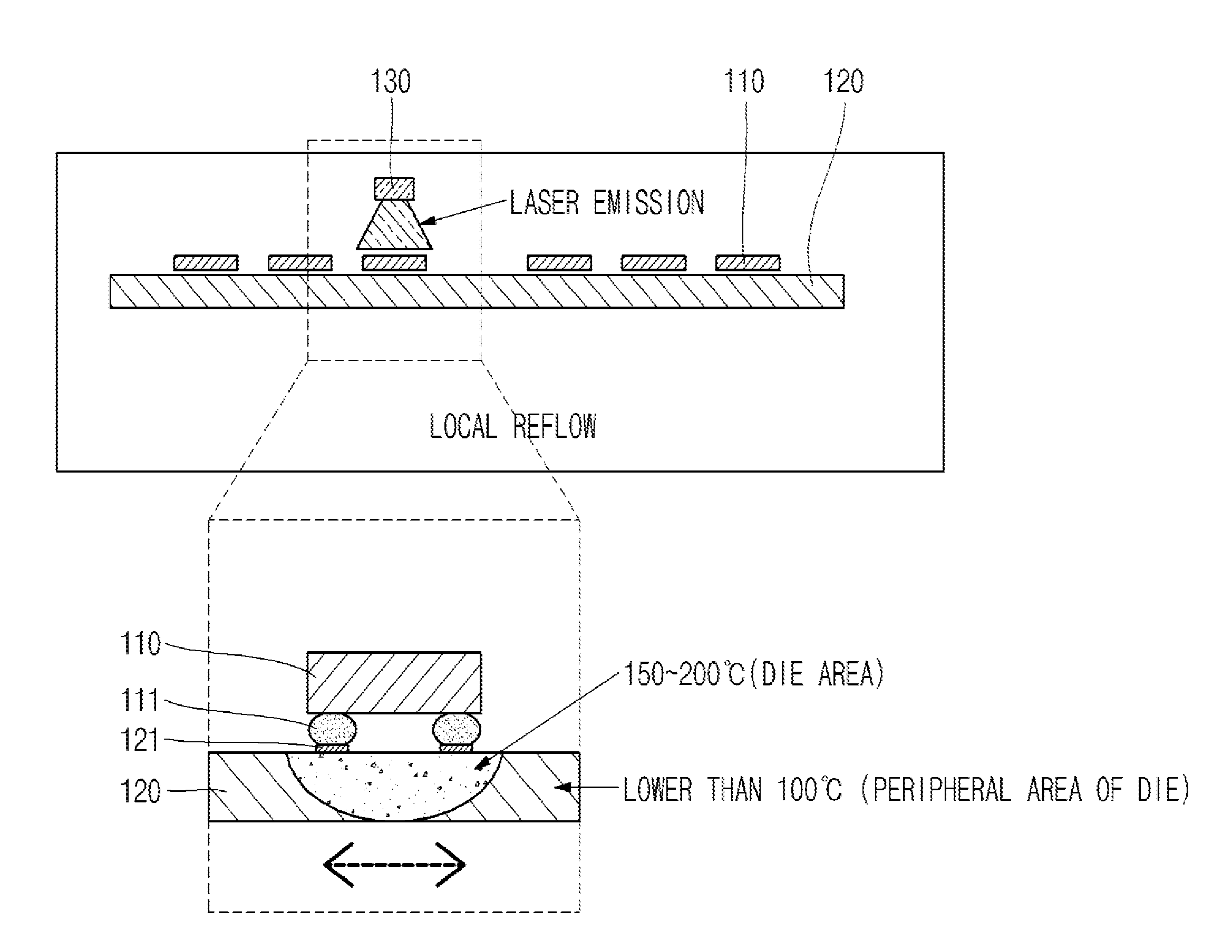
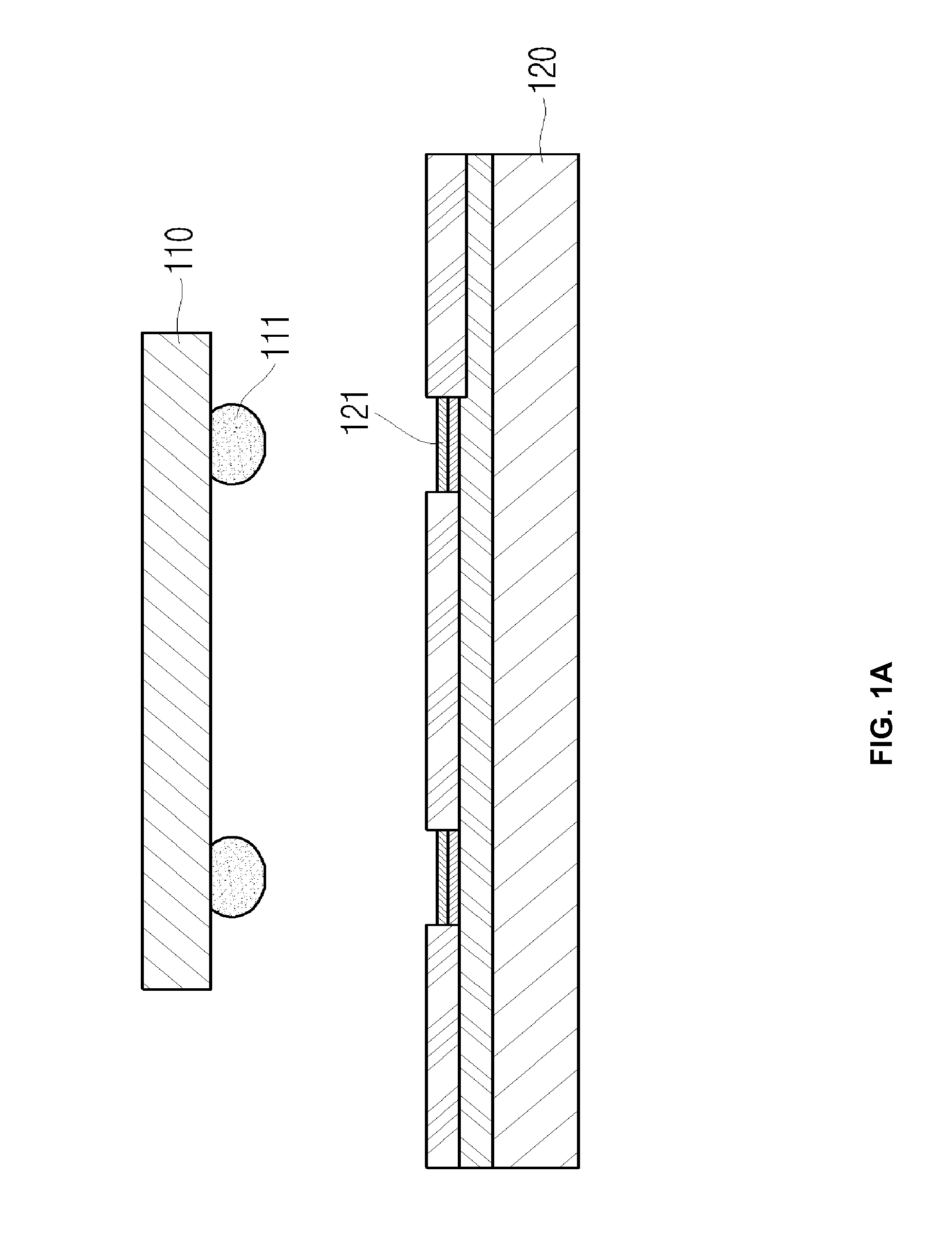
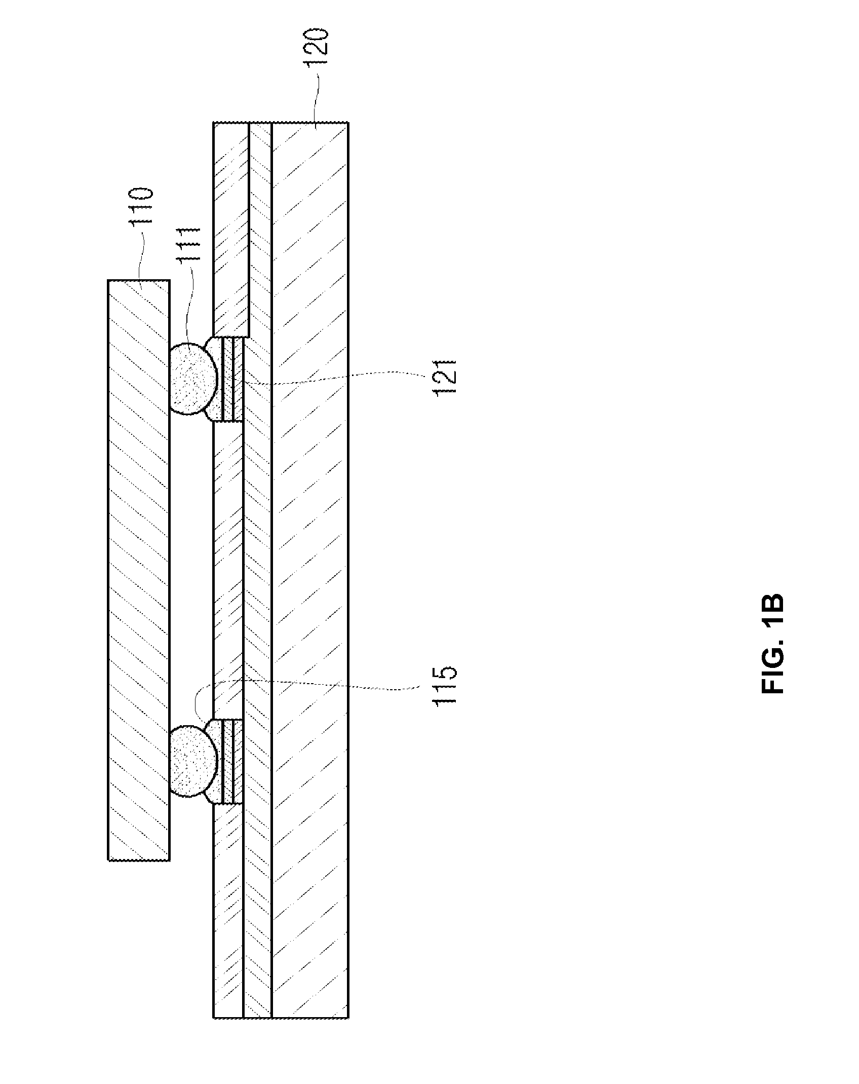
[0013]Certain aspects of the disclosure may be found in a method for laser assisted bonding for semiconductor die interconnections comprising forming flux on a circuit pattern on a circuit board, placing a semiconductor die on the circuit board where a bump on the semiconductor die contacts the flux, and reflowing the bump by directing a laser beam toward the semiconductor die. The laser beam may volatize the flux and make an electrical connection between the bump and the circuit pattern. A jig plate may be placed on the semiconductor die the laser beam is directed toward the semiconductor die. The jig plate may have an area that is approximately equal to that of the semiconductor die. Warpage may be reduced during heating or cooling of the semiconductor die by applying pressure to the jig plate. Jig bars may extend outward from the jig plate and may be in contact with the circuit board during the application of pressure to the jig plate. The jig plate may comprise one or more of: s...


PUM


Abstract

Laser assisted bonding for semiconductor die interconnections is disclosed and may, for example, include forming flux on a circuit pattern on a circuit board, placing a semiconductor die on the circuit board where a bump on the semiconductor die contacts the flux, and reflowing the bump by directing a laser beam toward the semiconductor die. The laser beam may volatize the flux and make an electrical connection between the bump and the circuit pattern. A jig plate may be placed on the semiconductor die when the laser beam is directed toward the semiconductor die. Warpage may be reduced during heating or cooling of the semiconductor die by applying pressure to the jig plate. Jig bars may extend outward from the jig plate and may be in contact with the circuit board during the application of pressure to the jig plate. The jig plate may comprise one or more of: silicon, silicon carbide, and glass.

Description

CROSS-REFERENCE TO RELATED APPLICATIONS[0001]The present application makes reference to, claims priority to, and claims the benefit of Korean Patent Application No. 10-2014-0105848, filed on Aug. 14, 2014, the contents of which are hereby incorporated herein by reference, in their entirety.FIELD[0002]Certain embodiments of the disclosure relate to semiconductor chip packaging. More specifically, certain embodiments of the disclosure relate to laser assisted bonding for semiconductor die interconnections.BACKGROUND[0003]In general, a semiconductor package includes a semiconductor die, a plurality of leads electrically connected to the semiconductor die and an encapsulant encapsulating the semiconductor die and the leads.[0004]A method for bonding a semiconductor die (e.g., in a flip chip configuration) and a circuit board using bumps generally includes providing a semiconductor die and a circuit board, jetting flux onto the circuit board, die-attaching for aligning bumps of the semic...

Claims


Application Information

Patent Timeline
IPC IPC(8): H01L23/00H05K3/34
CPCH01L24/81H05K3/3494H05K2203/107H01L2224/81201H01L2924/3511H01L2224/81815H01L24/75H01L2224/131H01L2224/13147H01L2224/16237H01L2224/75263H01L2224/75701H01L2224/75986H01L2224/81024H01L2224/81048H01L2224/81136H01L2224/81208H01L2224/81224H01L2924/351H01L2924/3512H01L2924/381H05K3/3436H05K2201/068H05K2201/10674H01L2924/014
Inventor RYU, DONG SULEE, CHOON HEUNGKIM, MIN HOKIM, CHOONG HOEYOON, JU HOONHWANG, CHAN HAJUNG, YANG GYOO
Owner AMKOR TECH SINGAPORE HLDG PTE LTD
Why Eureka
Try Eureka