

Sealing sheet, method for producing semiconductor device, and substrate with sealing sheet
a technology of sealing sheet and substrate, which is applied in the direction of adhesive articles, solid-state devices, synthetic resin layered products, etc., can solve the problems of voids and difficulty in adjustment, and achieve the effects of improving adhesion and semiconductor elements, high reliability, and improving adhesion and adhesion
Inactive Publication Date: 2016-02-25
NITTO DENKO CORP
View PDF1 Cites 4 Cited by
- Summary
- Abstract
- Description
- Claims
- Application Information
AI Technical Summary
Benefits of technology
The present invention provides a sealing sheet for improving the reliability of semiconductor devices. The sealing sheet has a special configuration that includes a thermosetting resin containing a liquid thermosetting resin and an under-fill material containing a flux agent. The use of this sealing sheet prevents rupture and improves the adhesion of the semiconductor element to the adherend while being easy to apply and efficiently meltable for reliable electrical connection. The production method of the sealing sheet also ensures that the semiconductor element is not contaminated during the process, resulting in improved reliability of the semiconductor device.
Problems solved by technology
As the sealing resin, liquid sealing resins are widely used, but in the case of liquid sealing resins, it is difficult to adjust the injection position and the injection amount, or the periphery of a bump having a reduced pitch cannot be sufficiently filled, and thus voids are generated.
Method used
View moreImage
Smart ImageViewing Examples

Examples
examples
[0140]Preferred Examples of the present invention will be illustratively described in detail below. However, for the materials, the blending amounts, and so on described in Examples, the scope of the present invention is not intended to be limited thereto unless definitely specified. The part(s) means “part(s) by weight”.
Login to View More PUM
| Property | Measurement | Unit |
|---|---|---|
| peel strength | aaaaa | aaaaa |
| peel strength | aaaaa | aaaaa |
| viscosity | aaaaa | aaaaa |
Abstract
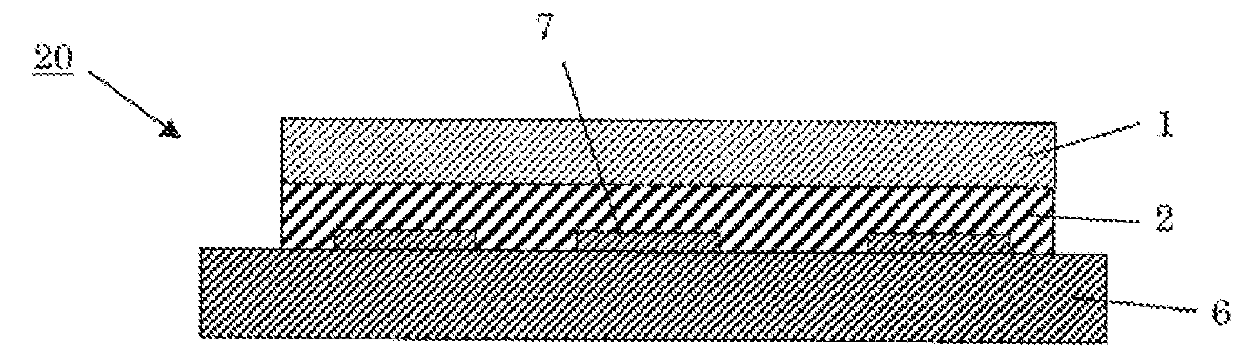
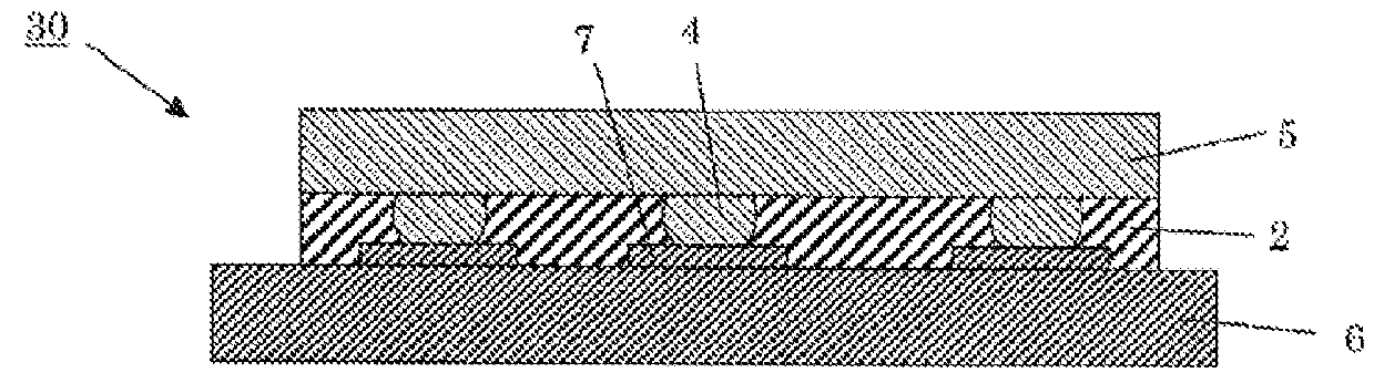
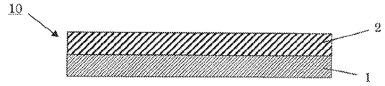
Provided are a sealing sheet capable of suppressing generation of voids due to satisfactory embeddability in irregularities of a semiconductor element or an adherend and with satisfactory workability before and after the sealing sheet is bonded to the adherend; a method for producing a semiconductor device using the sealing sheet; and a substrate with the sealing sheet bonded thereto. The sealing sheet includes a base material, and an under-fill material provided thereon having the following characteristics: a 90° peel strength from the base material of 1 mN / 20 mm or more and 50 mN / 20 mm or less; a rupture elongation of 10% or more at 25° C.; a minimum viscosity of 20,000 Pa·s or less at a temperature of 40° C. or more and 100° C. or less; and a minimum viscosity of 100 Pa·s or more at a temperature of 100° C. or more and 200° C. or less.
Description
TECHNICAL FIELD[0001]The present invention relates to a sealing sheet, a method for producing a semiconductor device, and a substrate with a sealing sheet.BACKGROUND ART[0002]In recent years, the demand for high density mounting associated with miniaturization and thinning of electronic instruments has been rapidly increased. In response to this demand, for semiconductor packages, the surface mounting type suitable for high density mounting has become mainstream in place of the conventional pin insertion type. Particularly, a flip chip mounting technique is developed in which a semiconductor chip and a substrate are electrically connected through a bump-shaped electrode (terminal) formed on the surface of the semiconductor chip.[0003]In surface mounting, a space between a semiconductor element and a substrate is filled with a sealing resin in order to protect the surface of the semiconductor element and secure connection reliability between the semiconductor element and the substrat...
Claims
Login to View More Application Information
Patent Timeline
 Patent Type & AuthorityApplications(United States)
IPC IPC(8): H01L23/00B32B7/12B32B27/36
CPCH01L24/83H01L24/81B32B2405/00B32B27/36H01L2224/8185B32B7/12H01L23/295H01L21/563H01L2224/73204H01L2224/83948H01L2224/271H01L2224/29318H01L2224/29371H01L2224/29324H01L2224/2939H01L2224/27334H01L24/13H01L24/14H01L24/16H01L24/27H01L24/29H01L24/32H01L24/73H01L24/92H01L2224/13025H01L2224/13111H01L2224/13144H01L2224/13147H01L2224/14181H01L2224/16145H01L2224/16227H01L2224/16245H01L2224/2919H01L2224/2929H01L2224/293H01L2224/29311H01L2224/29316H01L2224/29339H01L2224/29344H01L2224/29347H01L2224/29355H01L2224/29364H01L2224/29387H01L2224/29393H01L2224/32145H01L2224/32225H01L2224/32245H01L2224/81191H01L2224/81204H01L2224/81815H01L2224/83191H01L2224/83192H01L2224/83204H01L2224/83862H01L2224/8388H01L2224/9211H01L2224/92125H01L2924/15311H01L2224/27003H01L2224/2744H01L2924/15787H01L2224/16225B32B27/08B32B27/38H01L2224/81011H01L2224/83885B32B5/02B32B5/24B32B7/06B32B9/005B32B9/04B32B9/045B32B15/04B32B15/08B32B23/08B32B27/10B32B27/12B32B27/16B32B27/18B32B27/20B32B27/281B32B27/283B32B27/286B32B27/304B32B27/306B32B27/308B32B27/32B32B27/322B32B27/34B32B27/365B32B27/40B32B29/002B32B29/005B32B29/02B32B29/06B32B2255/02B32B2255/06B32B2255/10B32B2255/12B32B2255/205B32B2262/101B32B2307/50B32B2307/514B32B2307/748B32B2457/00B32B2457/08H01L2924/01006H01L2924/05442H01L2924/00014H01L2924/014H01L2924/01082H01L2924/01047H01L2924/01029H01L2924/0103H01L2924/01083H01L2224/81H01L2224/83H01L2924/00H01L2924/0635H01L2924/0665H01L2924/066H01L2924/095
InventorMORITA, KOSUKETAKAMOTO, NAOHIDE
OwnerNITTO DENKO CORP