
Super-junction structure and method for manufacturing the same and semiconductor device thereof

Active Publication Date: 2016-03-03
HANGZHOU SILICON-MAGIC SEMICON TECH CO LTD
View PDF13 Cites 12 Cited by
  • Summary
  • Abstract
  • Description
  • Claims
  • Application Information

AI Technical Summary

Benefits of technology

The present disclosure provides a super-junction structure that solves the problem of suppressing an avalanche current over conventional super-junctions. The structure includes first pillar regions with high doping concentration and low doping concentration sub-pillar regions, which change the path of the current and suppress the avalanche current even when a high voltage is applied. The structure has a high breakdown voltage and low on resistance. This makes the device less prone to damage. The method for manufacturing this structure is also provided.

Problems solved by technology

Thus, the conventional approach cannot take into account both a high breakdown voltage and a low on resistance.
A large voltage drop occurs across the base resistor RB and turns on the parasitic transistor, which in turn amplifies the avalanche current and damage the device.
Consequently, the conventional super-junction structure cannot really suppress an avalanche current even in a case that the super-junction structure is used as a drift region of the semiconductor device.

Method used


Image

  • Super-junction structure and method for manufacturing the same and semiconductor device thereof
  • Super-junction structure and method for manufacturing the same and semiconductor device thereof
  • Super-junction structure and method for manufacturing the same and semiconductor device thereof

Examples


Embodiment Construction

Brief Description of the Drawings

Detailed Description of Embodiments of the Invention

[0055]Reference will now be made in detail to particular embodiments of the disclosure in conjunction with appended drawings, so that objectives, features and advantages of the disclosure will become more apparent. For the purpose of clarity, some parts in the appended drawings are not drawn to scale. Further, for simplicity, a structure may be shown in one drawing while it may be actually obtained after several steps, and some well-known details may be omitted.

[0056]Some particular details will be described for thorough understanding of the present disclosure. However, the present disclosure may be practiced with or without these particular details by one skilled person, without departing the principles of the present disclosure. Thus, the present disclosure is not limited to the particular embodiments below.

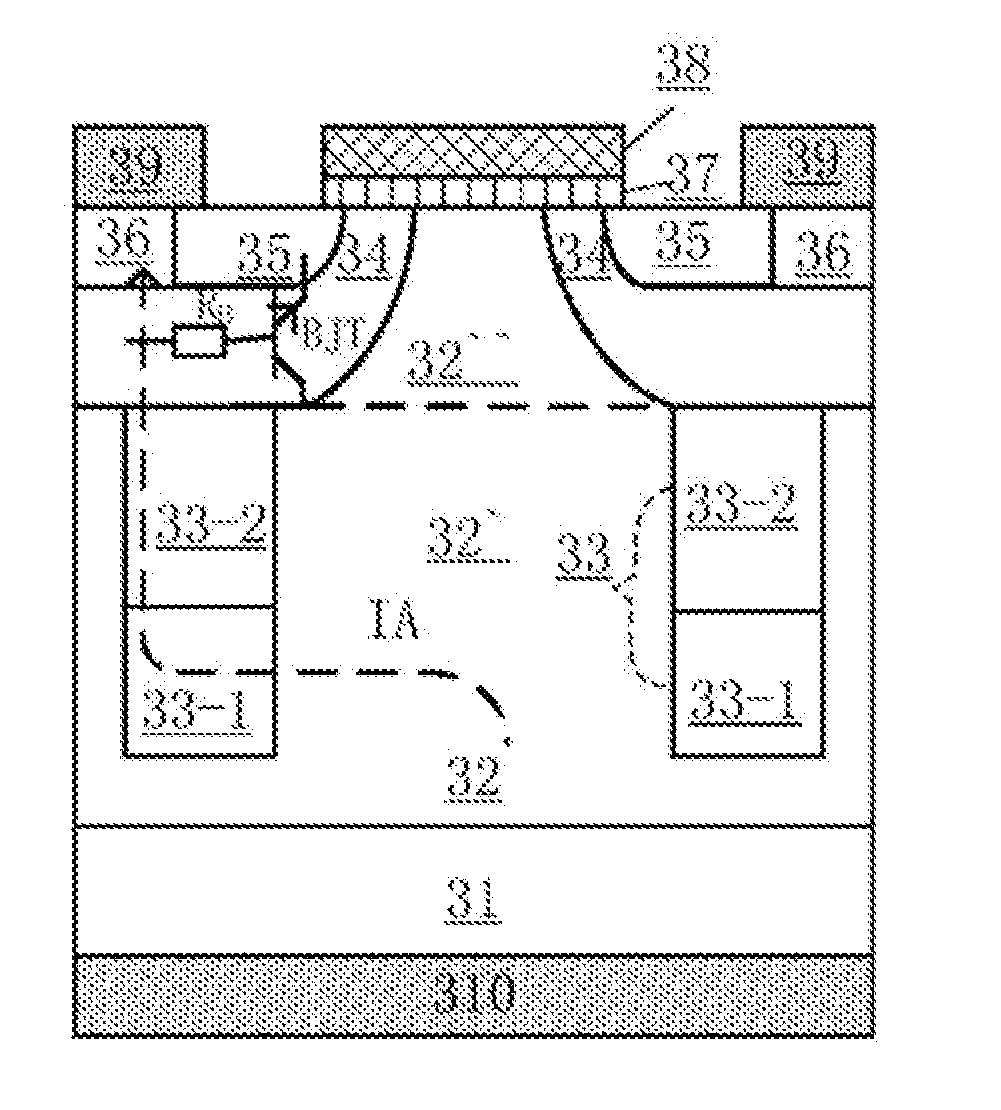
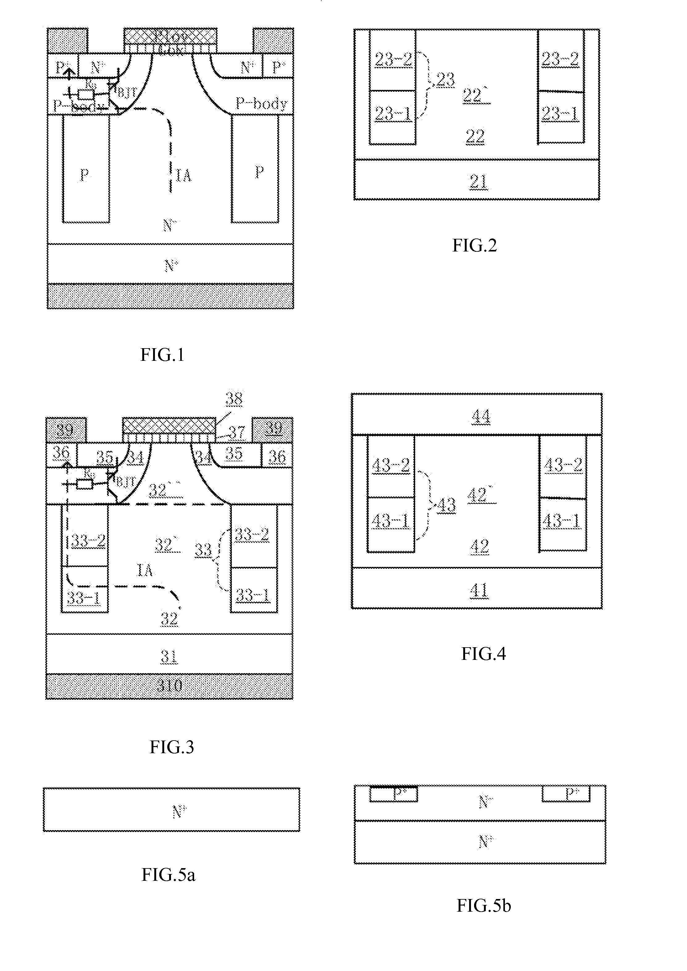
[0057]FIG. 2 is a structural diagram of a super-junction structure according to an embodime...


PUM


Abstract

The present disclosure relates to a super-junction structure, a method for manufacturing the super-junction structure and a semiconductor device including the super-junction structure. The super-junction structure includes an epitaxy layer of a first doping type and a plurality of first pillar regions of a second doping type which are formed in the epitaxy layer and are separated from each other. Each of the first pillar regions has a doping concentration that decreases from bottom to top. A portion of the epitaxy layer between adjacent ones of the first pillar regions is a second pillar region. The first pillar regions and the second pillar region are arranged alternatively to form the super-junction structure. The first pillar regions are characterized by the doping concentration that decreases from bottom to top so that the super-junction structure has a relatively high breakdown voltage and a relatively low on resistance. Moreover, the super-junction structure changes a path of an avalanche current and thus suppresses an avalanche current so that the device is not easily damaged.

Description

CLAIM OF PRIORITY[0001]This application claims priority to Chinese Application No. 201410441028.9, filed Sep. 1, 2014 (published as CN 10421376 A), which is hereby incorporated by reference.BACKGROUND OF THE DISCLOSURE[0002]1. Field of the Disclosure[0003]The present disclosure relates to semiconductor devices, and more particularly, to a super-junction structure, a method for manufacturing the super-junction structure and a semiconductor device including the super-junction structure.[0004]2. Description of the Related Art[0005]High-power semiconductor devices, such as metal-oxide-semiconductor field effect transistors (MOSFETs), insulated gate bipolar transistors (IGBTs) and the like, typically decreases a doping concentration of a drift region for a high breakdown voltage. However, the drift region will have a large on resistance if having a low doping concentration. Thus, the conventional approach cannot take into account both a high breakdown voltage and a low on resistance.[000...

Claims


Application Information

Patent Timeline
IPC IPC(8): H01L29/06H01L29/36H01L29/417H01L29/49H01L29/739H01L29/78
CPCH01L29/0634H01L29/7811H01L29/41741H01L29/36H01L29/4916H01L29/7395H01L29/66681H01L29/7823H01L29/1095H01L29/66333H01L29/7802
Inventor SUN, HELIAO, ZHONGPING
Owner HANGZHOU SILICON-MAGIC SEMICON TECH CO LTD
Learn More