
Dielectric film and dielectric element

a dielectric element and dielectric film technology, applied in the direction of fixed capacitors, stacked capacitors, fixed capacitor details, etc., can solve the problems of inability to describe the change in capacitance with temperature, difficult to resolve the problem, and limited manufacturing methods, etc., to improve the breakdown voltage, small temperature coefficient of capacitance, and high capacitance

Active Publication Date: 2016-03-17
TDK CORPARATION
View PDF2 Cites 0 Cited by
  • Summary
  • Abstract
  • Description
  • Claims
  • Application Information

AI Technical Summary

Benefits of technology

The present invention is related to a dielectric film for use in electronic devices. The film has a high dielectric constant and maintains its performance even at high temperatures. The film also has a low temperature coefficient of capacitance, which translates to better electric characteristics. The film contains specific components that facilitate the presence of other materials at grain boundaries, which improves its breakdown voltage. The technical effects of this invention include improved performance and reliability of electronic devices that use the dielectric film.

Problems solved by technology

However, when the laminated ceramic capacitor is embedded in an electronic circuit board, the thickness of the laminated ceramic capacitor and brittleness as a ceramic property cause the problem of producing, by the stress generated in an embedding process, cracks in the laminated ceramic capacitor or deformation in a portion of the electronic circuit board where the laminated ceramic capacitor is embedded.
It is difficult to resolve the problem even by a usual laminated ceramic capacitor having a very small shape.
However, a change in capacitance with temperature is not described, and a manufacturing method is limited.

Method used

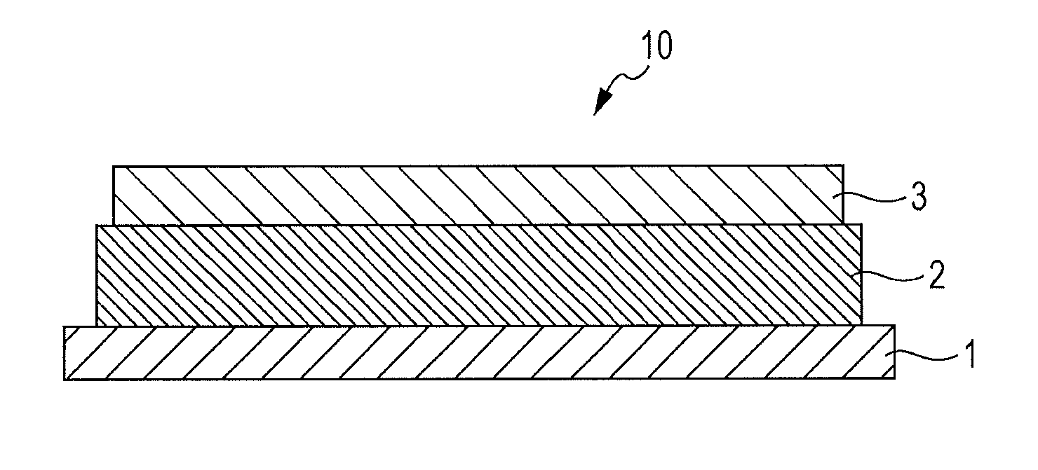

Image

  • Dielectric film and dielectric element
  • Dielectric film and dielectric element
  • Dielectric film and dielectric element

Examples


examples

[0048]The present invention is described in further detail below based on examples, but the present invention is not limited to these examples.

examples 19 to 33

[0069]First, a target for sputtering required for forming a dielectric film containing a main component represented by the general formula (Ba1-xCax)z(Ti1-yZry)O3 was produced by the same solid phase method as in Example 1. The mixing ratios of raw material powders of BaCO3, CaCO3, TiO2, ZrO2, V2O5, MnO, and CuO in the target were adjusted so as to obtain each of the dielectric film compositions shown in Table 1.

[0070]The dielectric film was formed by the same method as in Example 1 except that V2O5, MnO, and CuO were added to the target.

[0071]The resultant samples of Examples 19 to 33 were evaluated by the same method as in Example 1. The results are shown in Table 1.

Comparative Example 7

[0072]First, a target for sputtering required for forming a dielectric film containing a main component represented by the general formula (Ba1-xCax)z(Ti1-yZry)O3 was produced by the same solid phase method as in Example 1. The mixing ratios of raw material powders of BaCO3, CaCO3, TiO2, and ZrO2 i...

example 1 to example 17

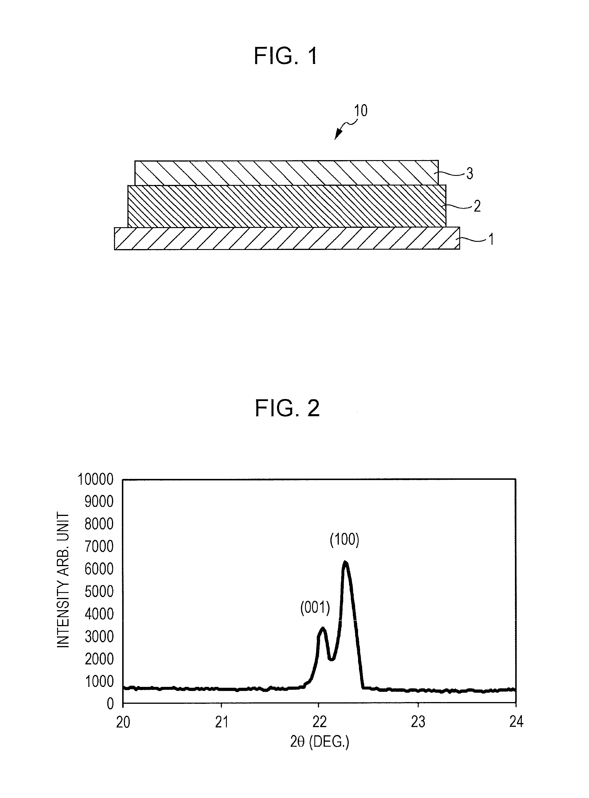
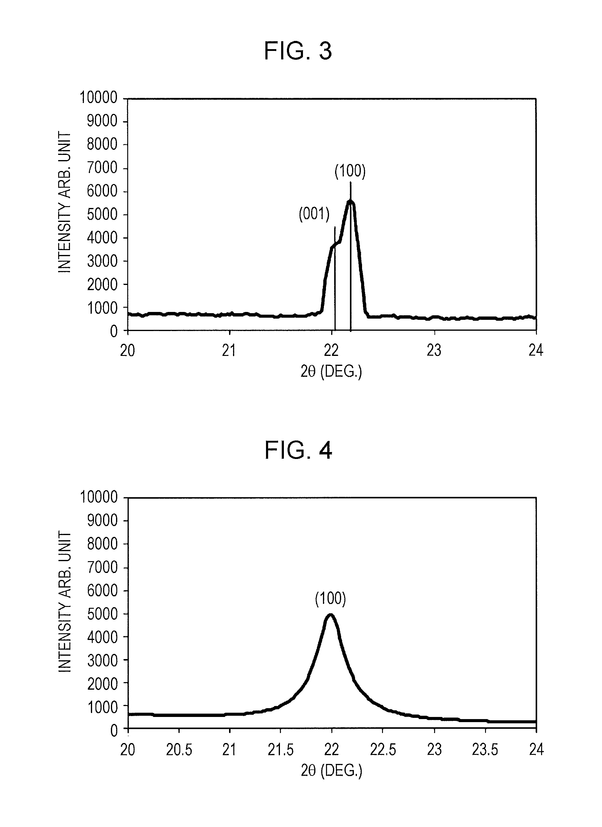
[0076]It can be confirmed by Table 1 that when the dielectric film contains as a main component a dielectric composition represented by the general formula (Ba1-xCax)z(Ti1-yZry)O3 wherein 0.001≦x≦0.400, 0.001≦y≦0.400, and 0.900≦zc−2θtt of a tetragonal structure represented by the general formula and the (100) plane diffraction peak position 2θc of a cubic structure represented by the general formula, the a small temperature coefficient of capacitance (TCC=within ±22%) can be realized while a dielectric constant of 1000 or more is exhibited.


PUM

PropertyMeasurementUnit
Angleaaaaaaaaaa
Substance countaaaaaaaaaa

Abstract

A dielectric film contains as a main component a dielectric composition represented by the general formula (Ba1-xCax)z(Ti1-yZry)O3 wherein 0.001≦x≦0.400, 0.001≦y≦0.400, and 0.900≦z<0.995. In an X-ray diffraction pattern of the dielectric composition, the dielectric composition has the relation 0.00°≦2θc−2θt<0.20° between (001) plane diffraction peak position 2θt of a tetragonal structure represented by the general formula and (100) plane diffraction peak position 2θc of a cubic structure represented by the general formula.

Description

BACKGROUND OF THE INVENTION[0001]1. Field of the Invention[0002]The present invention relates to a dielectric film and a dielectric element such as a thin-film capacitor, which includes the dielectric film.[0003]2. Description of the Related Art[0004]With multi-functionalization of electronic apparatuses, various functions are desired to be added to electronic circuit boards contained in electronic apparatuses. Therefore, the number of electronic components mounted on an electronic circuit board tends increase. Thus, there is strong demand for improving the mounting density of electronic components.[0005]One of the proposed answers to the demand is to embed electronic components in an electronic circuit board. One of the many electronic components mounted on an electronic circuit board is a usual laminated ceramic capacitor. However, when the laminated ceramic capacitor is embedded in an electronic circuit board, the thickness of the laminated ceramic capacitor and brittleness as a ...

Claims


Application Information

Patent Timeline
IPC IPC(8): H01G4/10H01G4/33
CPCH01G4/33H01G4/10H01G4/1227H01G4/20
Inventor TAKEDA, SAORIFURUKAWA, MASAHITOKOSUDA, MASANORISEZAI, YUJI
Owner TDK CORPARATION
Learn More