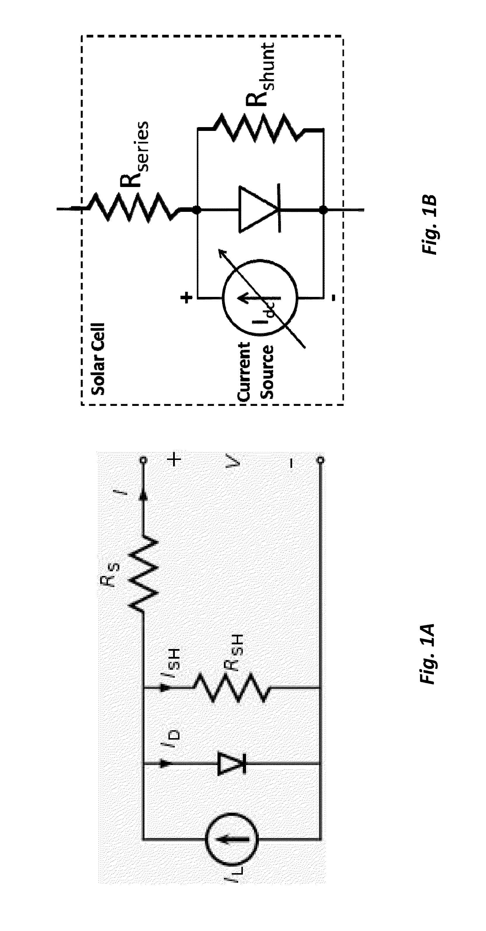
However, in actual realistic solar cells, the finite series resistance is due to the fact that a
solar cell has parasitic series resistance components in its
semiconductor and metallization (i.e., it is not a perfect conductor).
Such parasitic resistance components, including
semiconductor layer resistance and metallization resistance result in ohmic losses and power dissipation during the
solar cell operation.
The shunt resistance is caused by the undesirable leakage of current from one terminal to the other due to effects such as areal and edge
shunting defects as well as other non-idealities in the
solar cell.
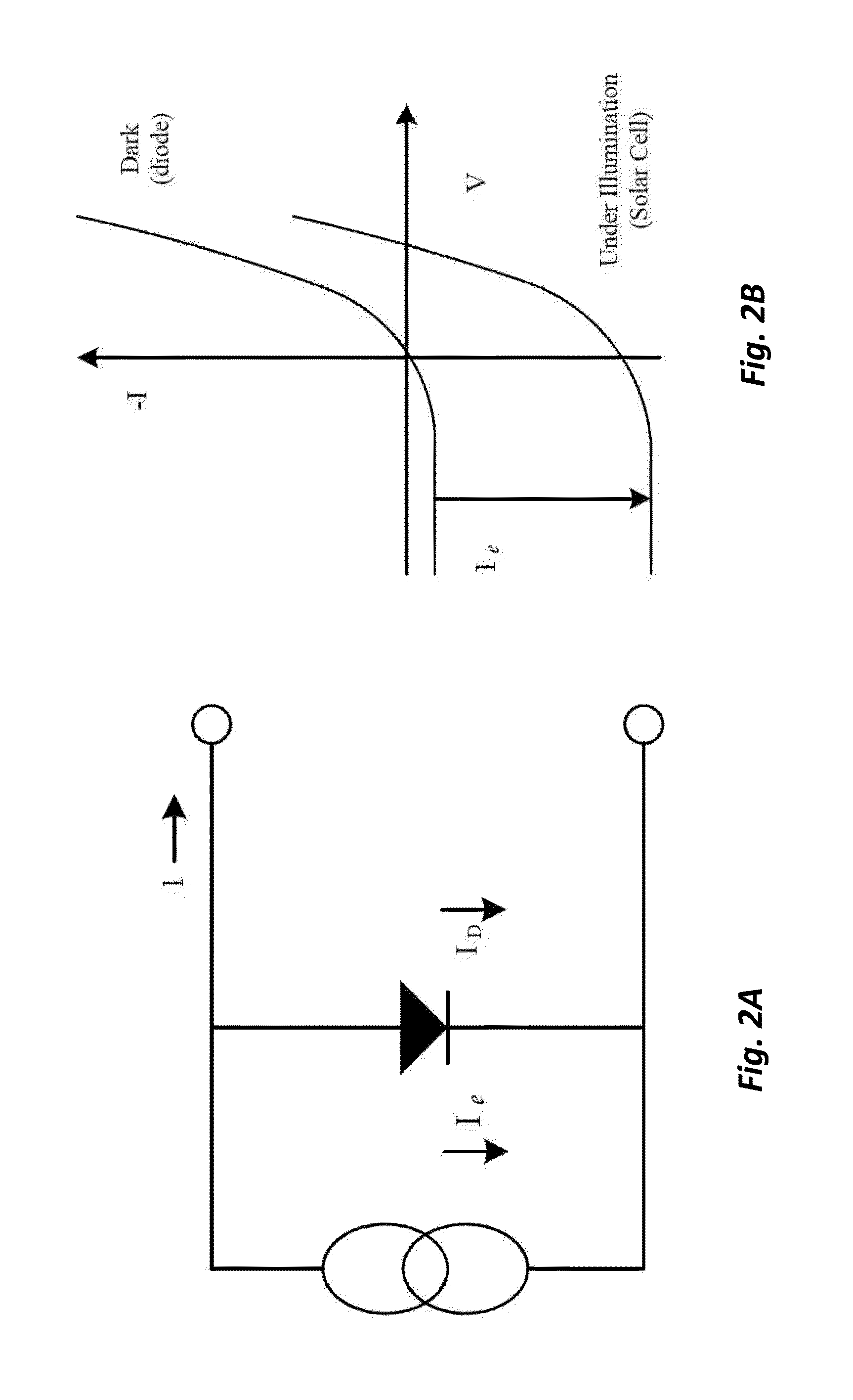
In a module with a plurality of solar cells, any shaded cells cannot produce the same amount of electrical power as the non-shaded cells within the PV module.
Under this
reverse bias condition the shaded
cell is consuming or dissipating significant power instead of producing power.
The power consumed and dissipated by the shaded or pratically shaded
cell will cause the cell to heat up, creating a localized hot spot where the shaded cell is located, and eventually possibly causing cell and module failure, hence creating major reliability failure problems in the field.
Unless appropriate precautions are taken, the power dissipation and the resulting localized heating of the shaded cell may result in poor cell and module reliability due to various failure
modes (such as failure of the reverse-biased shaded cell, failure of cell-to-cell interconnections, and / or failure of the module lamination materials such as the encapsulant and / or backsheet), as well as potential fire hazards in the installed PV systems.
Such hot-spot phenomena, which are caused by reverse biasing of the shaded cells, may permanently damage the affected PV cells and even cause fire hazards if the
sunlight arriving at the surface of the PV cells in a PV module is not sufficiently uniform (for instance, due to full or even partial shading of one or more cells).
While the external bypass diodes (typically three external bypass diodes included in the standard mainstream 60-cell
crystalline silicon PV module
junction box) protect the PV module and cells in case of shading of the cells, they can also actually result in significant loss of power harvesting and energy yield for the installed PV systems.
Moreover, the external
junction box may also be a source of field reliability failures and fire hazards in the installed PV systems.
This example still has the limitations of external bypass diodes, i.e., even when a single cell is shaded the bypass
diode shunts the entire
substring of cells with the shaded cell within the sub-string thus reducing the power harvesting and energy yield capability of the installed PV
system.
Again, this type of known PV module arrangement with external bypass diodes results in significant energy yield and power harvesting penalty for the installed PV systems in the field.
As a result, the electrical constraint of having all module strings connected in parallel operating at approximately the same
voltage does not allow a shaded string to activate its bypass diodes.
Therefore, in many cases, shade on PV modules in one of the strings may actually reduce the power produced by the entire string.
However, similar to previously described examples, these representative PV module installations suffer from the power harvesting limitation and reduced energy yield of the installed PV
system due to the problems outlined earlier.
In this example, the Schottky bypass
diode and the
compound semiconductor, multi junction solar cell are both on the same side (top side) of the solar cell, and have different material layer stacks, thereby making the
solar cell fabrication process much more complicated and costly (hence, such embodiment only demonstrated for the CPV application in which the CPV cells are quite expensive).
As a result of monolithic integration of the Schottky bypass
diode with the solar cell on the same expensive
germanium substrate, the overall
process complexity and cost are substantially and further increased while incurring an effective solar cell and solar panel efficiency penalty due to the integration of the Schottky bypass diode on the same side as the active sunnyside of the cell.
While such significant added
processing complexity and cost increase for fabrication of the solar cell may be acceptable in a CPV solar cell, it cannot be economically viable in a non-very
high concentration-CPV solar cell such as in
crystalline silicon solar cells. FIG. 11 is a diagram showing an example of monolithic integration of a bypass diode with a multi junction
compound semiconductor CPV cell.
In this example, the pn junction bypass diode and the compound
semiconductor, multi junction solar cell are both on the same side (top side) of the solar cell, and have different material stacks thereby making the
solar cell fabrication process much more complicated and costly (hence, such embodiment only demonstrated for the CPV application in which the CPV cells are quite expensive).
As a result of monolithic integration of the pn junction bypass diode with the solar cell on the same expensive
germanium substrate, the overall
process complexity and cost are and further increased while incurring an effective solar cell and solar panel efficiency penalty due to the integration of the bypass diode on the same side as the active sunnyside of the cell.
Again, this monolithic integration of the bypass pn junction diode on a front-contact compound semiconductor multi junction solar cell requires different stacks of material
layers in the solar cell and in the bypass switch, hence, substantially complicating the overall monolithic solar
cell processing, increasing the number of solar
cell fabrication process steps, and raising its manufacturing cost.
While such significant added
processing complexity and cost increase for fabrication of the solar cell may be acceptable in a CPV solar cell, it cannot be economically viable in a non-very
high concentration-CPV solar cell such as in
crystalline silicon solar cells.
In general, while the monolithic integration of the bypass diode (
Schottky diode or pn junction diode) as shown on an expensive multi junction solar cell for very
high concentration CPV applications may be acceptable for that particular application despite the extra cost and added manufacturing
process complexity of the monolithic integration with the solar cell, the approaches demonstrated for the expensive compound semiconductor multi junction solar cells would be prohibitively too expensive and not acceptable for mainstream flat-panel (non-concentrating or low to medium concentration) solar PV cells and modules.
Also, as noted previously, because the method of monolithic integration of the bypass diode consumes area otherwise used by the solar cell it reduces the effective
sunlight absorption and hence the effective cell efficiency due to loss of
sunlight absorption area.
However, this technology utilizes a module level / external converter box (micro-
inverter or DC-to-
DC converter) and associated interconnects technology which may cost around $30 to over $100 per PV module.
However, the module
level converter box is not and cannot be integrated with the individual cells, such as on cell backsides, and assembled with the individual cells.

