Non-volatile memory devices with thin-film and mono-crystalline silicon transistors

a technology of monocrystalline silicon and transistors, applied in semiconductor devices, instruments, electrical appliances, etc., can solve the problem of large “read latency” and achieve the effect of efficient drive bit lines and fast sensing of stored data

Inactive Publication Date: 2016-04-07
SCHILTRON
View PDF0 Cites 3 Cited by
  • Summary
  • Abstract
  • Description
  • Claims
  • Application Information

AI Technical Summary

Benefits of technology

[0009]According to one embodiment of the present invention, a non-volatile memory device combines thin-film transistor-based memory cells with bulk mono-crystalline silicon transistors, which can more efficiently drive bit lines for fast sensing of the stored data in the thin-film memory cells.

Problems solved by technology

As the time required to sense the data on the bit lines is substantial, a large “read latency” results.

Method used


Image

  • Non-volatile memory devices with thin-film and mono-crystalline silicon transistors
  • Non-volatile memory devices with thin-film and mono-crystalline silicon transistors
  • Non-volatile memory devices with thin-film and mono-crystalline silicon transistors

Examples


Embodiment Construction

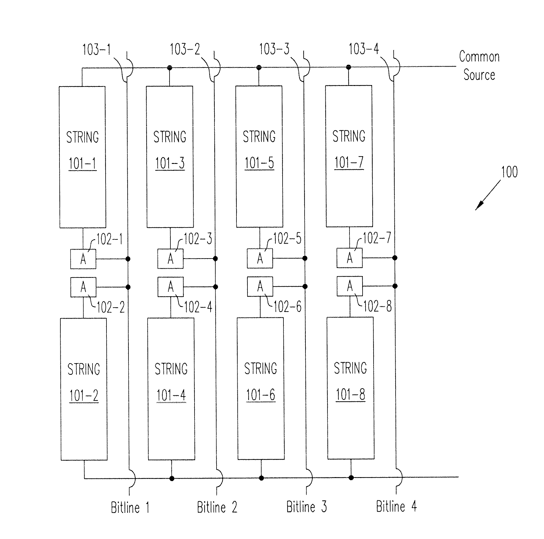
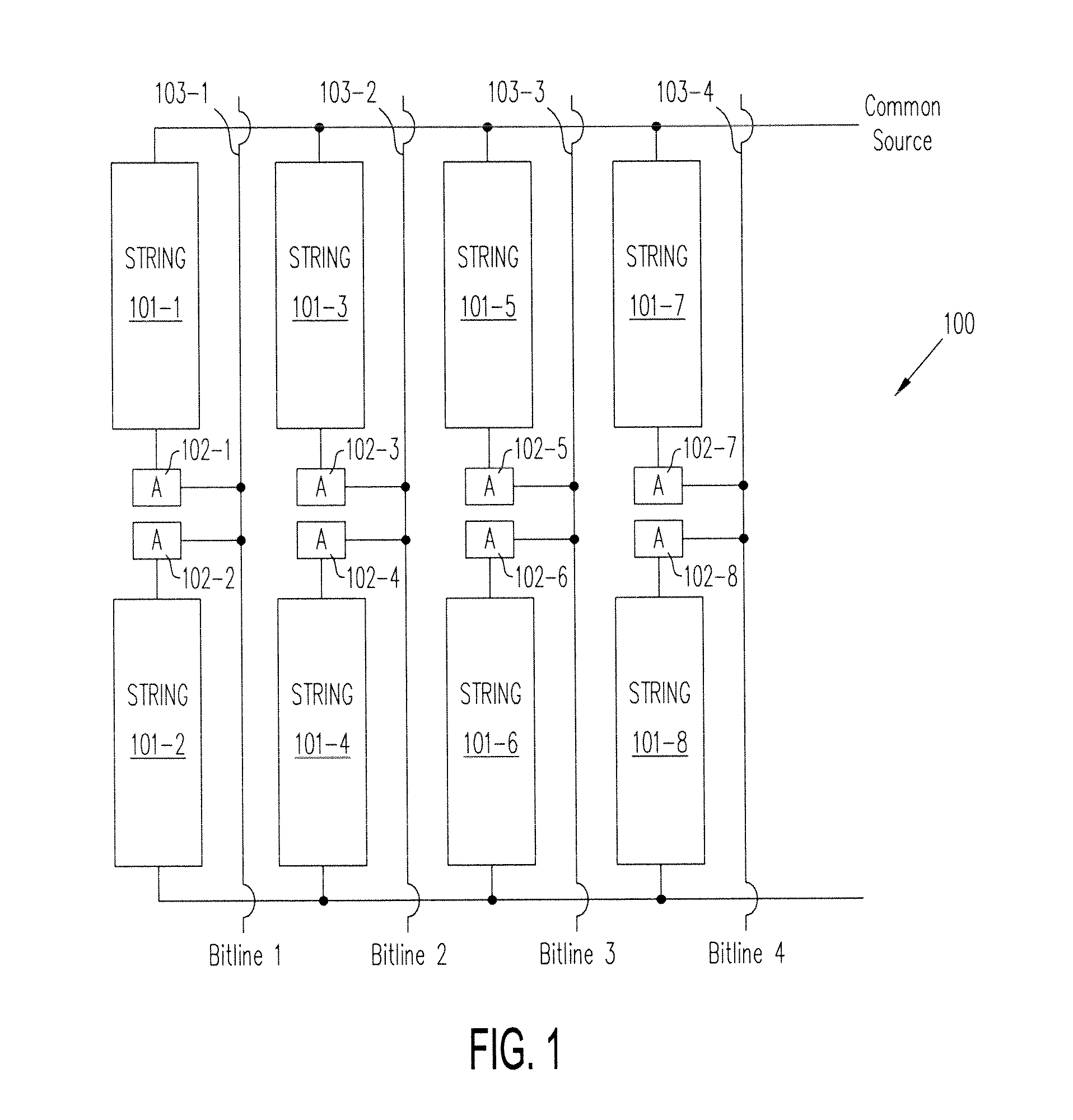
[0023]FIG. 1 is a block diagram illustrating non-volatile memory array 100 provided according to one embodiment of the present invention. The non-volatile memory array may include dual-gate thin-film devices or transistors as non-volatile storage devices. Each dual-gate device may include a floating gate as one of the gate elements in the dual-gate device. In some embodiments, floating gates may be used as both of the gate elements in the dual-gate device. The floating gate may be implemented by a small-dimension thin film conductor (e.g., less than 20 nanometers thick or on each side). The thin-film conductor may be formed out of any suitable material, such as titanium nitride (TiN), tantalum nitride (TaN), doped polysilicon, or any combination thereof. Alternatively, the floating gate may be provided in a dielectric layer embedded with conductor nanodots, also known as nanocrystals.

[0024]As shown in FIG. 1, thin-film transistor-based nonvolatile memory strings 101-1 to 101-8 are r...


PUM


Abstract

A non-volatile memory device combines thin-film transistor-based memory cells with bulk mono-crystalline silicon transistors, which can more efficiently drive bit lines for fast sensing of the stored data in the thin-film memory cells.

Description

CROSS-REFERENCE TO RELATED APPLICATIONS[0001]The present application is related to and claims priority of U.S. provisional patent application (“Copending Provisional application”), Ser. No. 62 / 060,115, entitled “Non-Volatile Memory Devices with Thin-Film and Mono-Crystalline Silicon Transistors,” filed on Oct. 6, 2014. The Copending Provisional patent application is hereby incorporated herein by reference in its entirety.BACKGROUND OF THE INVENTION[0002]1. Field of the Invention[0003]The present invention relates to non-volatile memory designs. In particular, the present invention relates to thin-film transistor-based nonvolatile memory devices that include bulk mono-crystalline silicon transistors.[0004]2. Discussion of the Related Art[0005]The typical thin-film transistor has a much lower electrical current-driving capability than a similarly sized transistor formed in the mono-crystalline bulk of a silicon wafer because of the disordered structure in the thin-film transistor's ch...

Claims


Application Information

Patent Timeline
Patent Type & Authority Applications(United States)
IPC IPC(8): H01L29/786H01L29/16H01L29/423H01L27/115H01L29/49
CPCH01L29/78645H01L27/11524H01L27/11529H01L29/16H01L29/4908H01L29/42372H01L27/11551G11C16/0483G11C16/26H10B41/41H10B41/20H10B43/40H10B43/20
Inventor WALKER, ANDREW J.
Owner SCHILTRON
Why Eureka
Try Eureka