10T Non-Volatile Static Random-Access Memory

a random access memory and non-volatile technology, applied in the field of semiconductor memories, can solve the problems of loss of data in the sram cell, loss of data in the nvsram circuit, and large capacity of computer systems and portable electronic devices such as tablets and smart phones

Active Publication Date: 2016-04-21
INFINEON TECH LLC
View PDF7 Cites 4 Cited by
  • Summary
  • Abstract
  • Description
  • Claims
  • Application Information

AI Technical Summary

Problems solved by technology

Computer systems and portable electronic devices such as tablets and smart phones require large capacity, high speed volatile and non-volatile storage of data.
Interruption of the power supply source causes loss of the data in the SRAM cell.
One disadvantage of present nvSRAM circuits is their limited density and relatively large memory cell size, typically including 12 or more transistors per nvSRAM cell.
If power is removed from the volatile charge storage circuit 102, the data will be lost.

Method used


Image

  • 10T Non-Volatile Static Random-Access Memory
  • 10T Non-Volatile Static Random-Access Memory
  • 10T Non-Volatile Static Random-Access Memory

Examples


Embodiment Construction

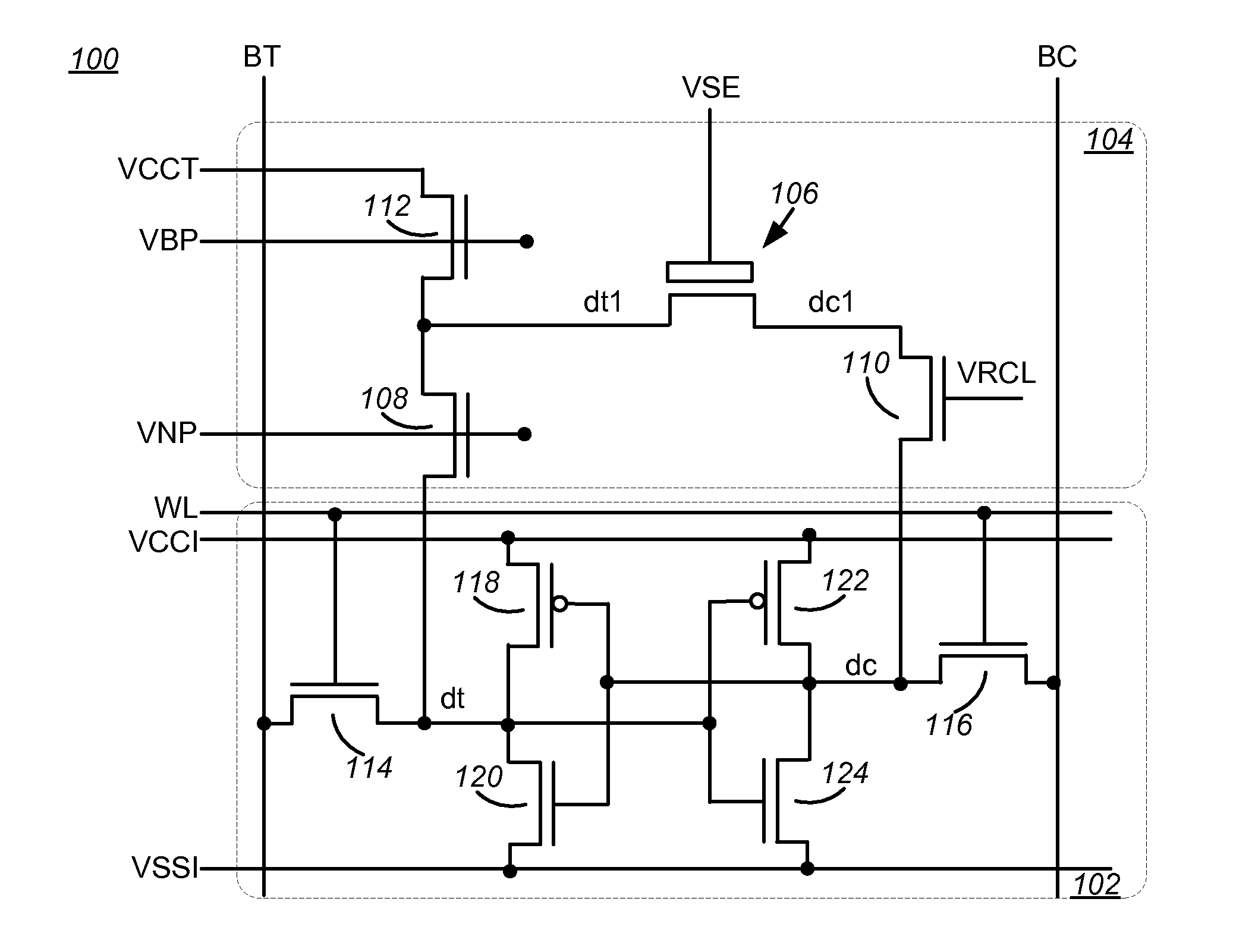
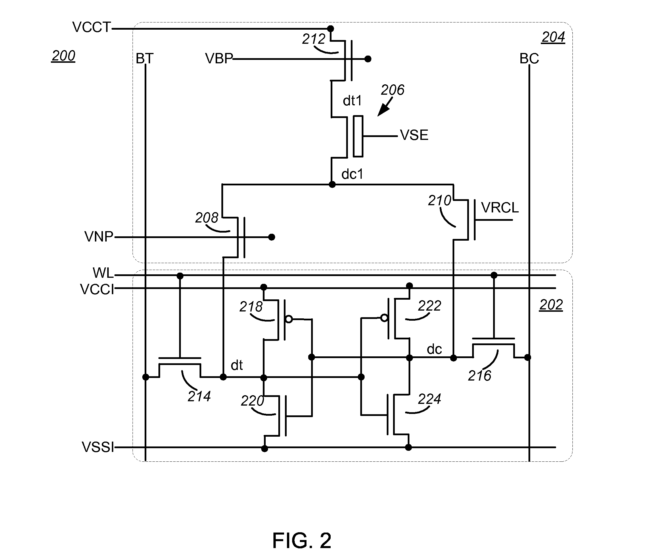
[0020]The present disclosure is directed generally to semiconductor memories and more particularly to a memory including a volatile charge storage circuit, and a non-volatile charge storage circuit including or consisting of exactly one non-volatile memory (NVM) element, and methods of operating the same to recall non-inverted data from the non-volatile charge storage circuit for every RECALL operation.

[0021]In the following description, for purposes of explanation, numerous specific details are set forth in order to provide a thorough understanding of the present invention. It will be evident, however, to one skilled in the art that the present invention may be practiced without these specific details. In other instances, well-known structures, and techniques are not shown in detail or are shown in block diagram form in order to avoid unnecessarily obscuring an understanding of this description.

[0022]Reference in the description to “one embodiment” or “an embodiment” means that a p...


PUM


Abstract

A memory including an array of nvSRAM cells and method of operating the same are provided. Each nvSRAM cell includes a volatile charge storage circuit, and a non-volatile charge storage circuit including exactly one non-volatile memory (NVM) element, a first transistor coupled to the NVM element through which data true is coupled to the volatile charge storage circuit, a second transistor coupled to the NVM element through which a complement of the data is coupled to the volatile charge storage circuit and a third transistor through which the NVM element is coupled to a positive voltage supply line (VCCT). In one embodiment, the first transistor is coupled to a first node of the NVM element, the second transistor is coupled to a second node of the NVM element and the third transistor is coupled between the first node and VCCT. Other embodiments are also disclosed.

Description

CROSS-REFERENCE TO RELATED APPLICATIONS[0001]This application claims the benefit of priority under 35 U.S.C. 119(e) to U.S. Provisional Patent Application Ser. No. 62 / 066,770, filed Oct. 21, 2014, which is incorporated by reference herein in its entirety.TECHNICAL FIELD[0002]This disclosure relates generally to semiconductor memories and more particularly to a Non-Volatile Static Random-Access Memory (nvSRAM) including nvSRAM cells having a reduced number of transistors and methods of operating the same.BACKGROUND[0003]Computer systems and portable electronic devices such as tablets and smart phones require large capacity, high speed volatile and non-volatile storage of data. Present types of semiconductor memory that use a combination of specialized volatile and non-volatile technologies. One type of volatile memory is static random-access memory (SRAM) which is often implemented using a bistable transistor flip-flop or a latching circuit. The word “static” indicates that the memor...

Claims


Application Information

Patent Timeline
Patent Type & Authority Applications(United States)
IPC IPC(8): G11C14/00G11C16/14G11C16/04
CPCG11C14/0063G11C16/14G11C16/0466G11C16/0408G11C11/419
Inventor TANDINGAN, JOSEPH S.ASHOKKUMAR, JAYANTSTILL, DAVIDSIMAN, JESSE J.
Owner INFINEON TECH LLC
Why Eureka
Try Eureka