
Method for concurrent system management and error detection and correction requests in integrated circuits through location aware avoidance logic

a technology of avoidance logic and integrated circuit, applied in the field of memory systems and architectures, can solve the problems of large increase in the number of cosmic ray interactions, memory errors will accumulate, and the negative impact of active data scrubbing on system bandwidth, and simplify the design of the memory interface. , the effect of simplifying the data integrity management uni

Active Publication Date: 2016-04-28
CAES COLORADO SPRINGS LLC
View PDF9 Cites 5 Cited by
  • Summary
  • Abstract
  • Description
  • Claims
  • Application Information

AI Technical Summary

Benefits of technology

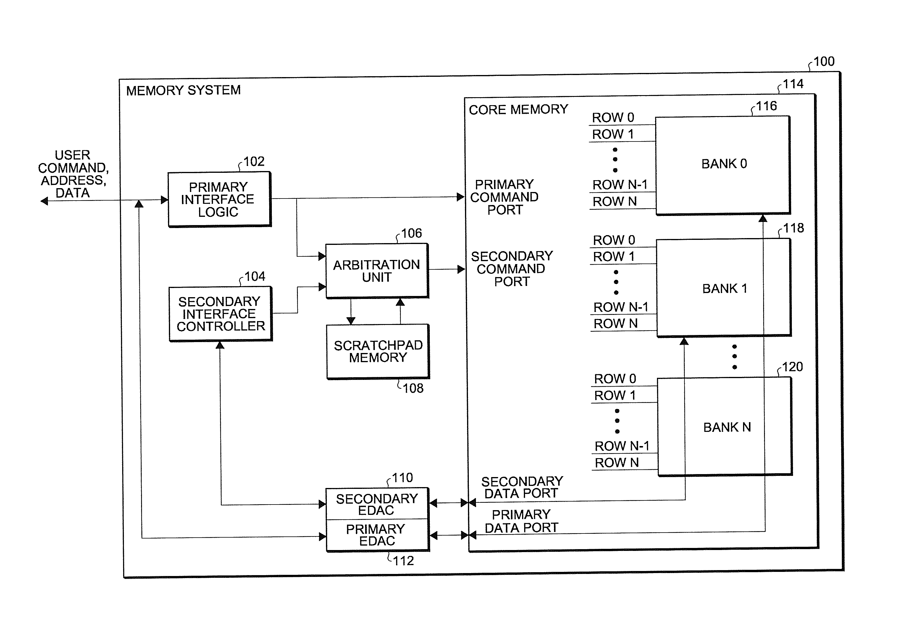
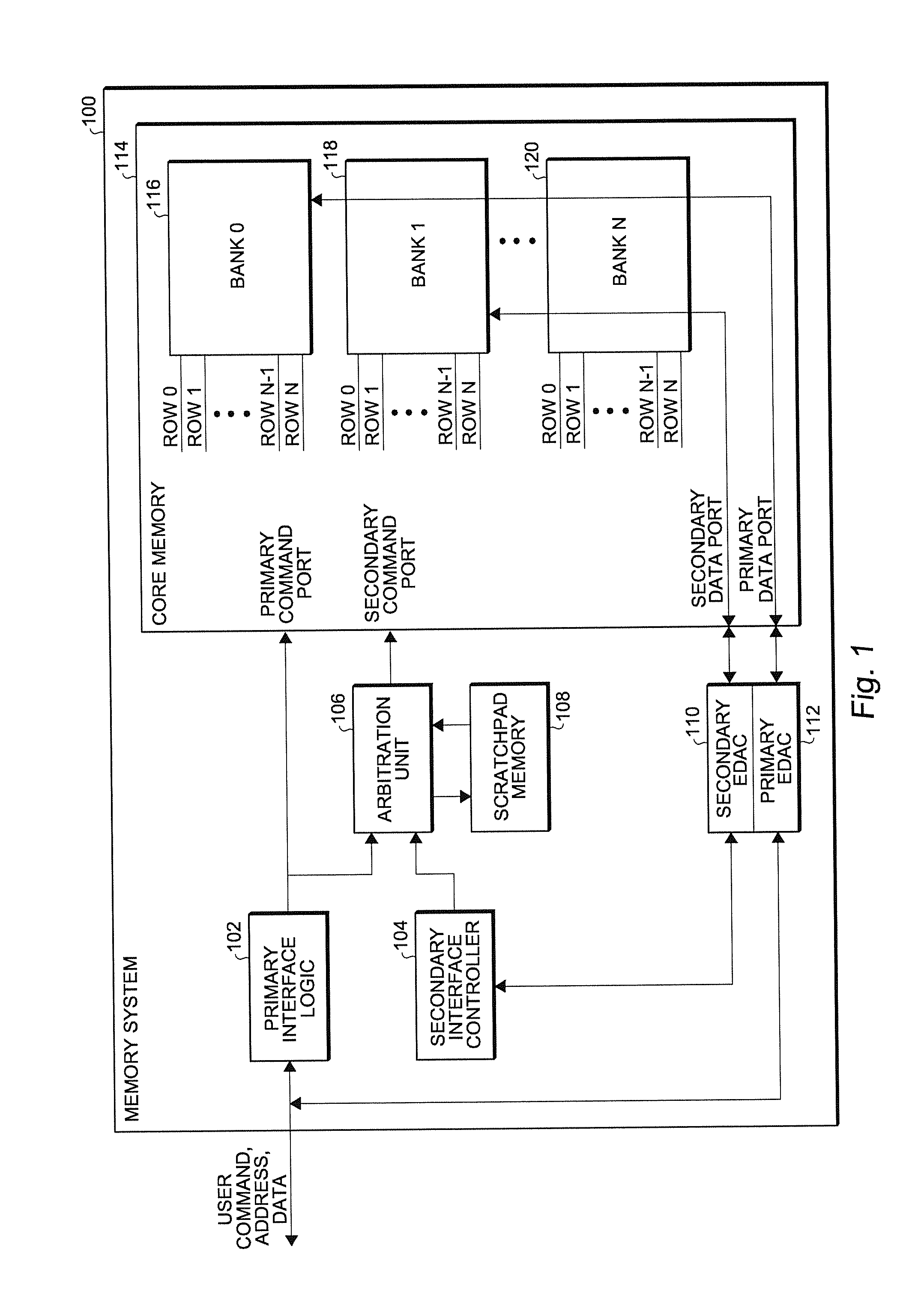
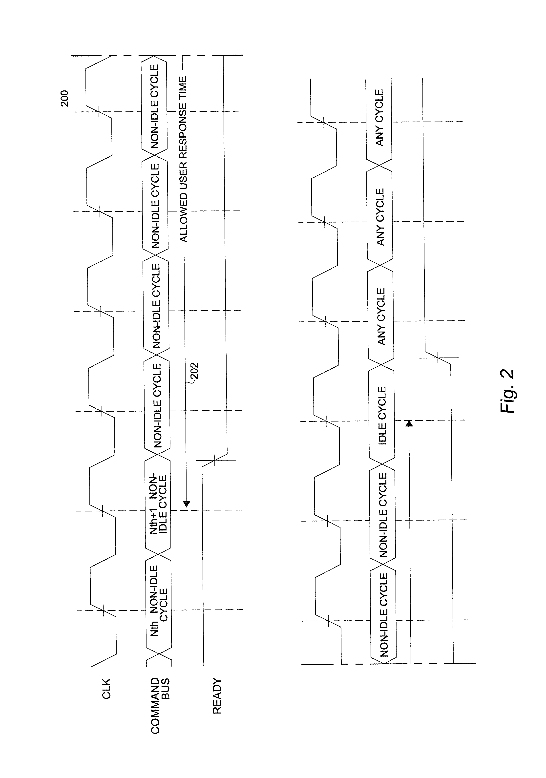
The present invention provides a method and system for incorporating active error correction inside a memory device. This method completely hides memory scrub cycles from the end user, reducing the impact on system bandwidth and simplifying the design of the memory interface and data integrity management unit. An arbitration unit is implemented to eliminate overlapping memory requests and ensure data integrity. A data bus secondary to the primary user data bus is implemented for any type of on-chip background activity. The method dynamically tracks recently scrubbed memory locations and locations which were skipped due to primary / secondary conflicts, avoiding the need for a large scratchpad memory. The method provides improved memory bandwidth and simplifies user interface design requirements. The system uses location aware secondary interface logic, reducing the required additional circuitry.

Problems solved by technology

If the memory is used in a harsh environment such as high altitude or even space environments, the problem is greatly exacerbated as the number of cosmic ray interactions increases dramatically.
In this type of implementation, memory errors will accumulate until the data is requested by the user.
Further, it is the user's responsibility to write the corrected data back to the memory, or the data resident in the memory device risks incurring an additional error, which would result in an uncorrectable error condition for conventional Hamming Codes.
Other error correction methods have been described; however, all result in significant area and performance penalties.
In a memory device this is undesirable.
This approach consumes device bandwidth as the user must execute periodic read-modify-write operations to correct the failing data bits as they occur.
Depending upon the rate of data corruption and the size of the memory, this impact can be very significant.
Finally, the design complexity required to incorporate this approach into end user systems is significant.

Method used


Image

  • Method for concurrent system management and error detection and correction requests in integrated circuits through location aware avoidance logic
  • Method for concurrent system management and error detection and correction requests in integrated circuits through location aware avoidance logic
  • Method for concurrent system management and error detection and correction requests in integrated circuits through location aware avoidance logic

Examples


Embodiment Construction

[0010]A semiconductor memory—whether it is SRAM, DRAM, NAND Flash, NOR Flash or some other form of memory—is typically laid out in rows and columns. These rows and columns are typically further organized in banks. One or more bits of information are accessed by selecting a particular bank, row, and column (a memory address). The electrical pathway upon which the data flows from the memory location will be referred to below as the bus and the circuitry that interprets the address into a selected bank, row and column will be referred to as the decode circuitry.

[0011]Error Detection and Correction (EDAC) refers to a method well known in the industry that uses extra data bits (called check bits) to store information that can detect and correct an error in the primary data. A Hamming code is one common implementation of this concept. For example, in a Hamming code, the addition of three check bits to a four bit data word would allow single error correction and double error detection (SEC...


PUM


Abstract

A method of incorporating active error correction inside a memory device is used, whereby memory scrub cycles can be completely hidden from an end user. The method simplifies the design of the memory interface and simplifies the data integrity management unit for the end user. An arbitration unit is implemented to allow concurrent processing of primary (user) and secondary (scrub) requests. The arbitration unit is location aware in context to the primary interface and is responsible for eliminating overlapping memory requests.

Description

FIELD OF THE INVENTION[0001]The present invention relates to memory systems and architectures, and more particularly to a memory device incorporating active error correction inside the memory device, whereby the memory scrub cycles can be completely hidden from the end user.BACKGROUND OF THE INVENTION[0002]It is well documented that data bits in a memory device can be flipped by the occurrence of a terrestrial cosmic ray as it interacts with a memory cell. If the memory is used in a harsh environment such as high altitude or even space environments, the problem is greatly exacerbated as the number of cosmic ray interactions increases dramatically. In an effort to reduce the soft error rate of memory devices, error detection and correction (EDAC) is often employed. In a typical system implementation, this EDAC is passive; that is, data is verified and corrected only when requested by the user. In this type of implementation, memory errors will accumulate until the data is requested b...

Claims


Application Information

Patent Timeline
IPC IPC(8): G06F11/10G06F3/06
CPCG06F11/1076G06F3/0673G06F3/064G06F3/0619G06F2211/1088G06F11/106G06F11/1004G06F11/108
Inventor MNICH, CHRISTOPHERMABRA, JONATHANVON THUN, MATTHEW
Owner CAES COLORADO SPRINGS LLC
Learn More