

Hybrid Vapor Phase-Solution Phase Growth Techniques for Improved CZT(S,Se) Photovoltaic Device Performance
a photovoltaic device and growth technique technology, applied in the field of hybrid vapor phase-solution phase growth technique for improving czt(s, se)based photovoltaic devices, can solve the problems of device not showing improvement in voc, film suffers from pinholes, and the voltage of open circuit increases
- Summary
- Abstract
- Description
- Claims
- Application Information
AI Technical Summary
Benefits of technology
Problems solved by technology
Method used
Image

Examples
Embodiment Construction
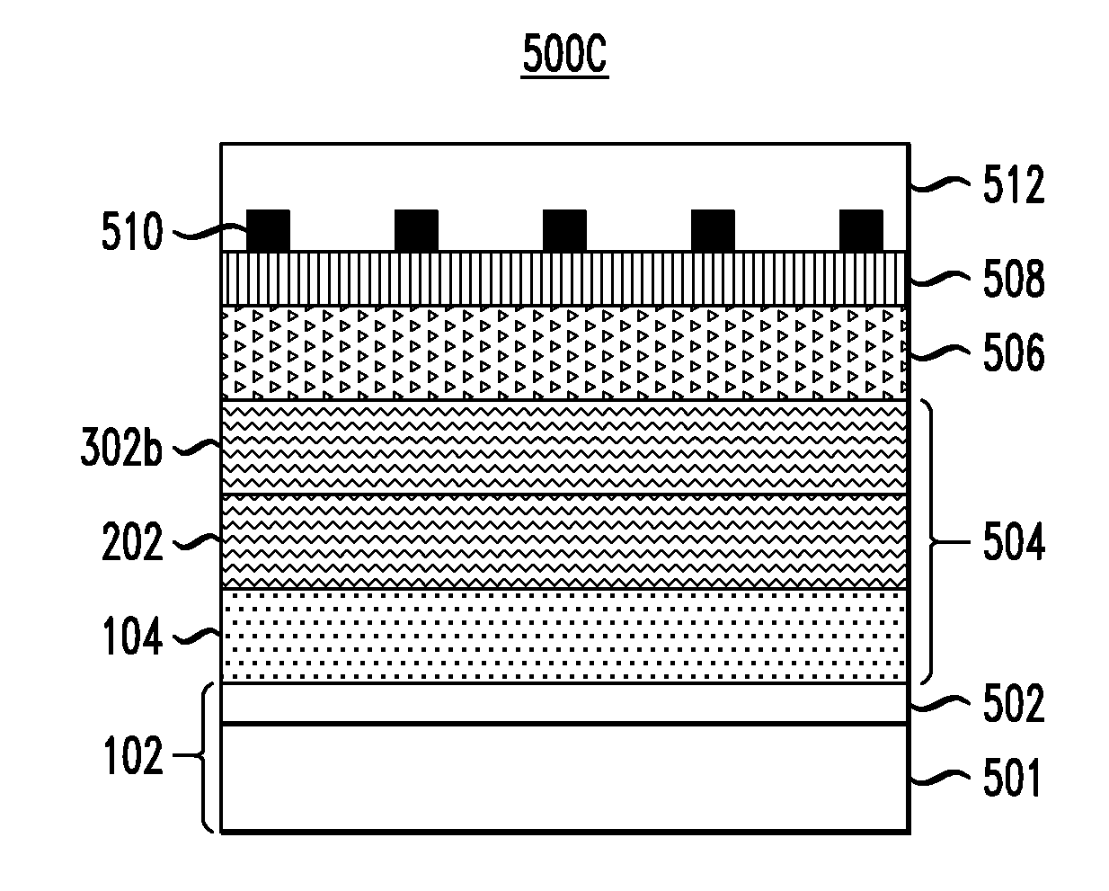
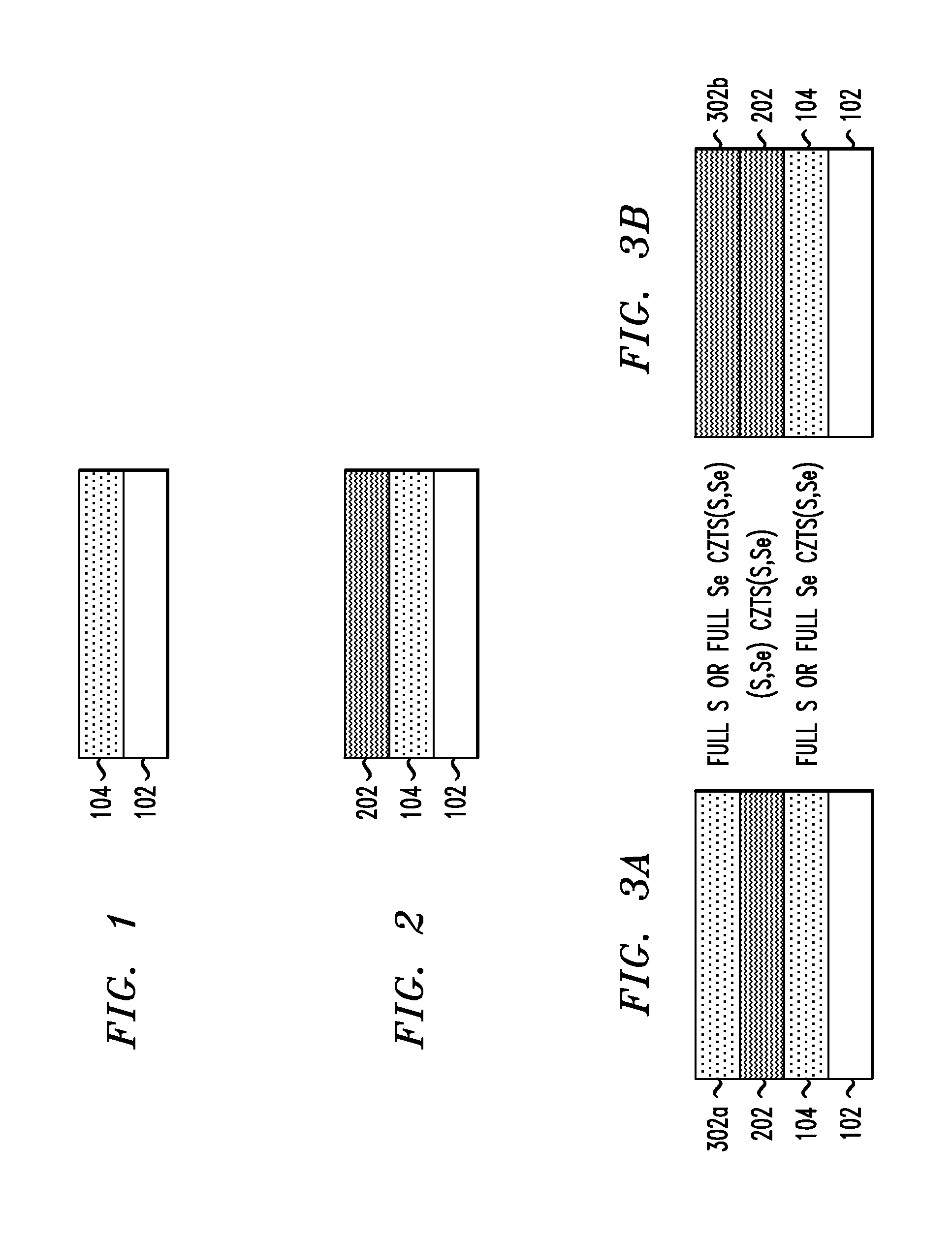
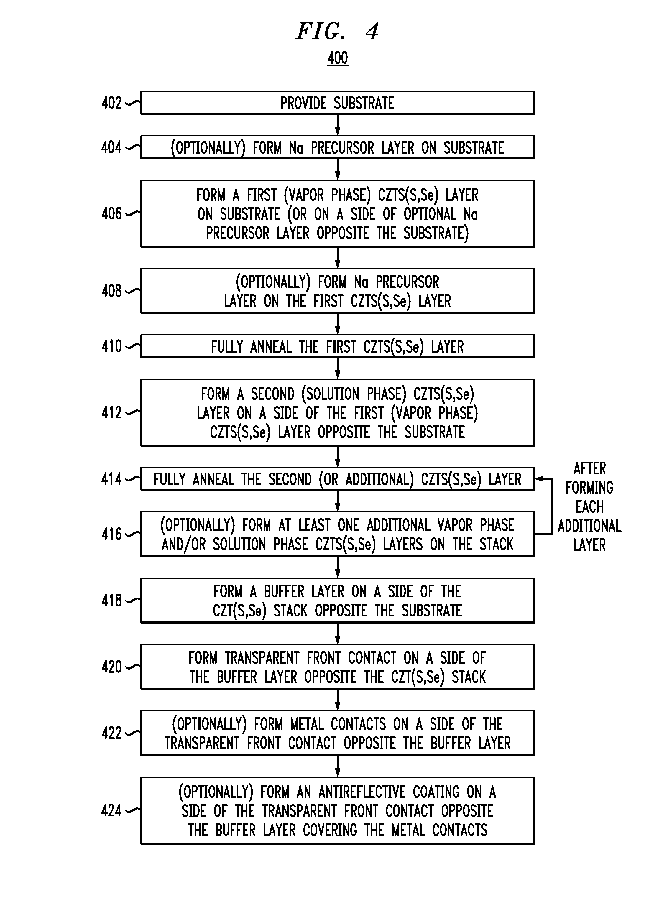
[0022]As provided above, while CZT(S,Se)-based photovoltaic devices have been produced with efficiencies at or above 12% using solution phase techniques, defects in the resulting film such as pinholes can lead to shorting of the device when conductive contacts are added. Vapor deposition can be used to produce pinhole-free CZT(S,Se) films. However, the resulting devices have efficiencies well below that achieved with solution phase processing.
[0023]As also provided above, it may be desirable to employ electron blocking layers or hole transport layers for improved rectifying behavior and open circuit voltage (Voc). However, these hole transport materials are often formed from oxides such as tungsten trioxide (WO3), nickel oxide (NiO), or molybdenum trioxide (MoO3). All of these materials are easily (undesirably) reduced by hydrazine which is commonly employed in solution phase deposition.
[0024]Advantageously, provided herein are hybrid vapor phase-solution phase CZT(S,Se) deposition ...
PUM
| Property | Measurement | Unit |
|---|---|---|
| pressure | aaaaa | aaaaa |
| temperature | aaaaa | aaaaa |
| thickness | aaaaa | aaaaa |
Abstract
Description
Claims
Application Information