
Scanning Electron Microscope

a scanning electron microscope and electron microscope technology, applied in the field of scanning electron microscope, can solve the problems of inability to achieve high resolution and increase chromatic aberration, and achieve the effect of reducing the effect of shading

Active Publication Date: 2016-05-26
HITACHI HIGH-TECH CORP
View PDF3 Cites 14 Cited by
  • Summary
  • Abstract
  • Description
  • Claims
  • Application Information

AI Technical Summary

Benefits of technology

The present invention relates to a method and apparatus for simultaneously acquiring secondary electron and backscattered electron images using a scanning electron microscope (SEM). By arranging detectors and adjusting the arrangement of the solid angle of a passing hole, shading caused by the detectors can be reduced during high magnification factor observation, while the detection of signals that travel in an off-axis direction and are not detected by the detectors can be improved during low magnification factor observation. This allows for an SEM that reduces the effect of shading in a broad magnification factor range. Additionally, by positioning a detector closer to the sample side and shaping its sensitive surface to be axisymmetrical with reference to the optical axis, the detection of backscattered electrons can be improved compared to conventional SEM.

Problems solved by technology

In an ordinary SEM, the chromatic aberration increases in a low-acceleration region, and a high resolution cannot be achieved.

Method used


Image

  • Scanning Electron Microscope
  • Scanning Electron Microscope
  • Scanning Electron Microscope

Examples


first embodiment

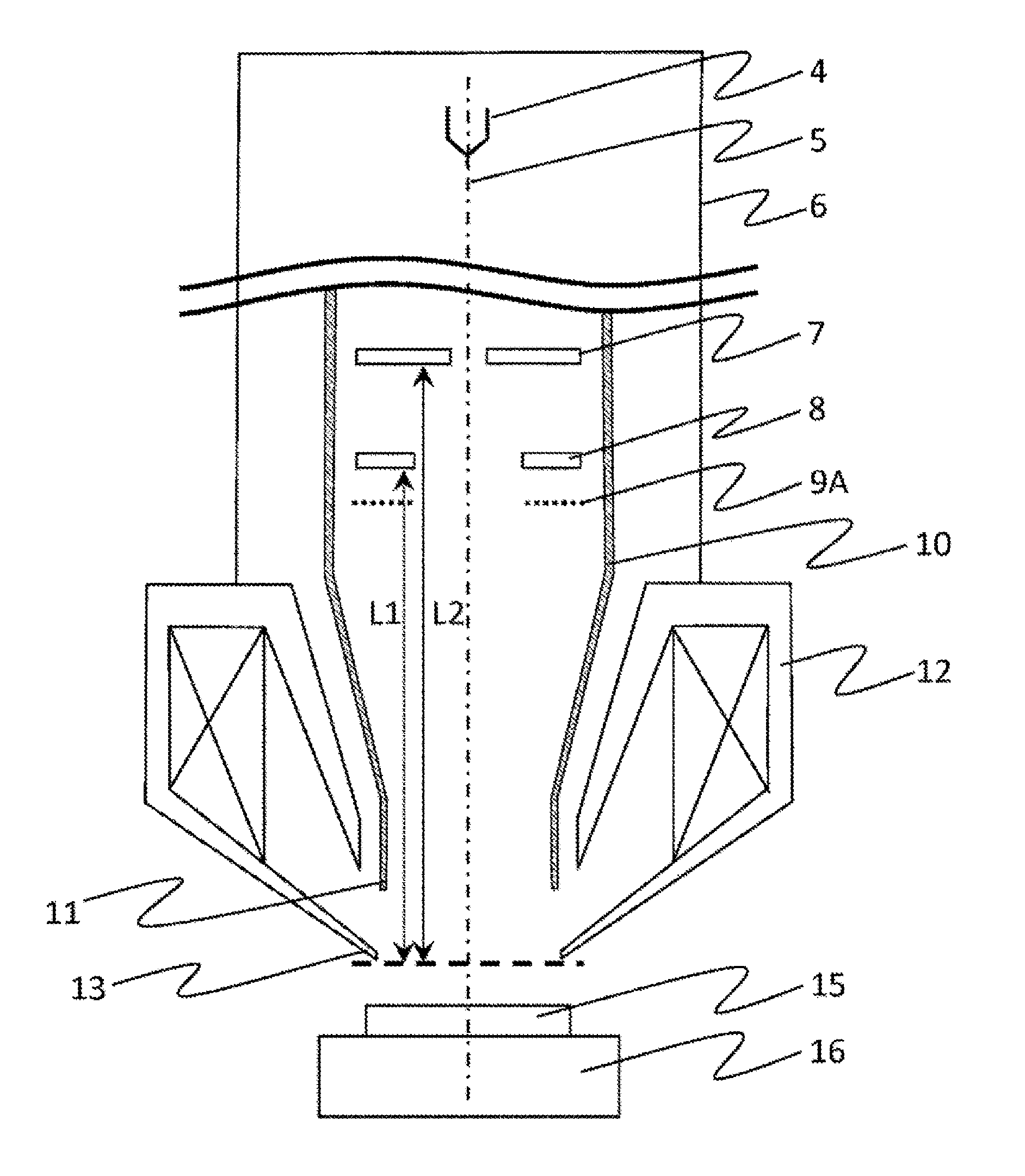
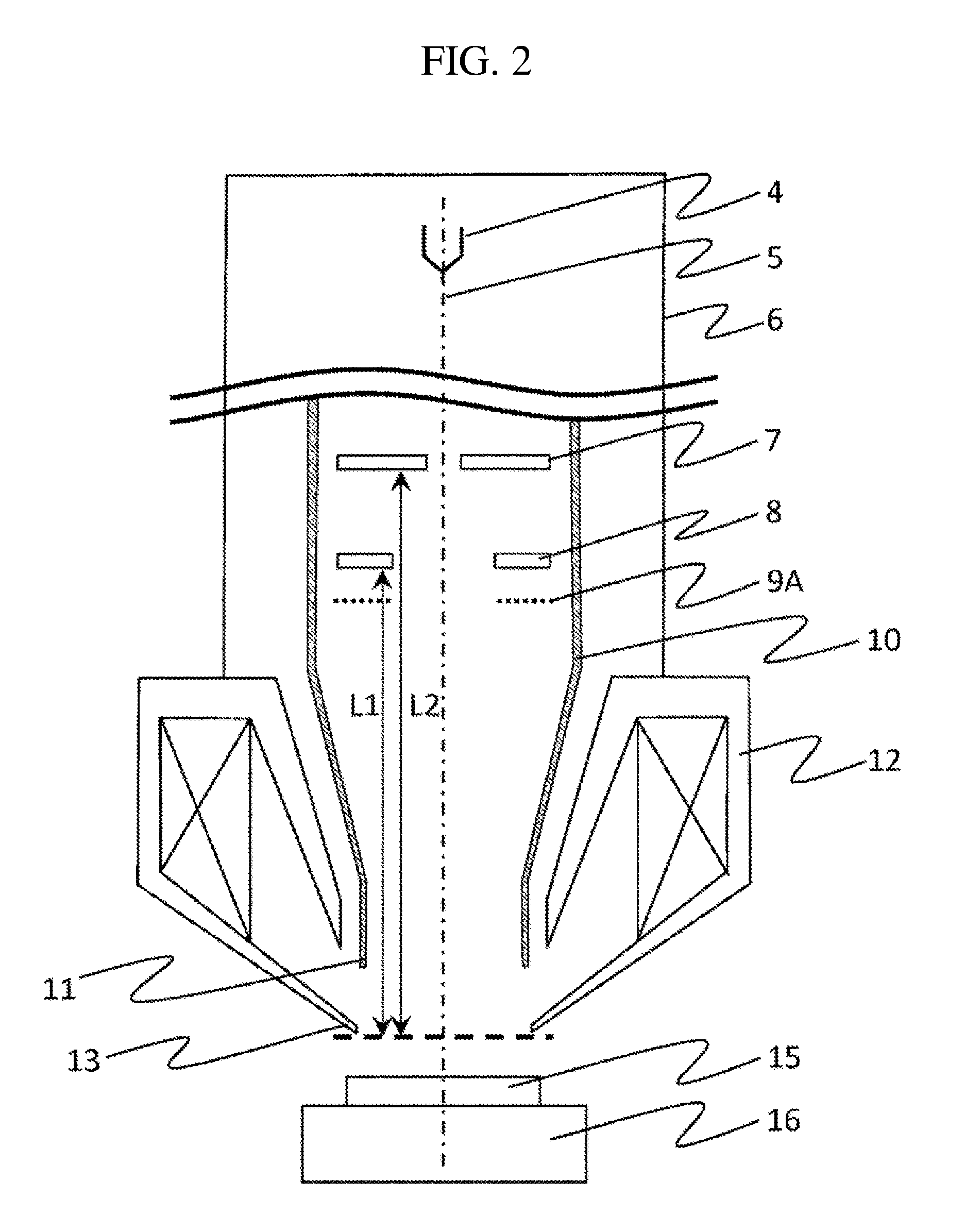
[0054]FIG. 2 illustrates a conceptual diagram of the overall configuration of a scanning electron microscope according to this embodiment. The scanning electron microscope illustrated in FIG. 2 largely includes: an electron gun 4 with a mechanism to irradiate an irradiation electron beam to a sample 15; an aperture directed to limiting the diameter of the irradiation electron beam; an electron lens, such as a condenser lens or objective lens; a detector directed to mainly detecting a secondary electron 2; a detector directed to mainly detecting a backscattered electron 3; an energy filter 9A directed to shielding the secondary electron 2; a deflector; a controller that controls a sample stand 16 on which the sample 15 is placed and which moves the sample 15 and determines an observation region, the mechanism of the sample stand 16, SEM image display equipment, and the entire SEM; and a vacuum exhaust facility. The position of the sensitive surface of the detector where each signal e...

second embodiment

[0078]FIG. 6 illustrates a conceptual diagram of the overall configuration of the scanning electron microscope according to this embodiment. The main differences from the first embodiment are hereinafter described:

[0079]The scanning electron microscope illustrated in FIG. 6 broadly includes: the electron gun 4; an aperture; a condenser lens; an objective lens; a second detector; a first detector; the energy filter 9A; a deflector; the sample 15; a controller that controls the sample stand 16 and the mechanism of the sample stand 16, an SEM image display device, and the entire SEM; and a vacuum exhaust facility.

[0080]The type of the objective lens of the scanning electron microscope of FIG. 6 is different from the type of the objective lens according to the first embodiment. The objective lens according to this embodiment is of a semi-in-lens type intended to leak a magnetic field to the sample. The resolution thereby achieved is higher than that achieved in the configuration of the ...


PUM


Abstract

This scanning electron microscope is provided with: a deceleration means that decelerates an electron beam (5) when the electron beam is passing through an objective lens; and a first detector (8) and a second detector (7) that are disposed between the electron beam and the objective lens and have a sensitive surface having an axially symmetric shape with respect to the optical axis of the electron beam. The first detector is provided at the sample side with respect to the second detector, and exclusively detects the signal electrons having a high energy that have passed through a retarding field energy filter (9A). When the distance between the tip (13) at the sample side of the objective lens and the sensitive surface of the first detector is L1 and the distance between the tip at the sample side of the objective lens and the sensitive surface of the second detector is L2, then L1 / L2≦5 / 9. As a result, when performing low-acceleration observation using a deceleration method by means of a scanning electron microscope, it is possible to detect signal electrons without the effect of shading in a magnification range of a low magnification on the order of hundreds of times to a high magnification of at least 100,000×. Also, it is possible to highly efficiently detect backscattered electrons, of which the amount generated is less than that of secondary electrons.

Description

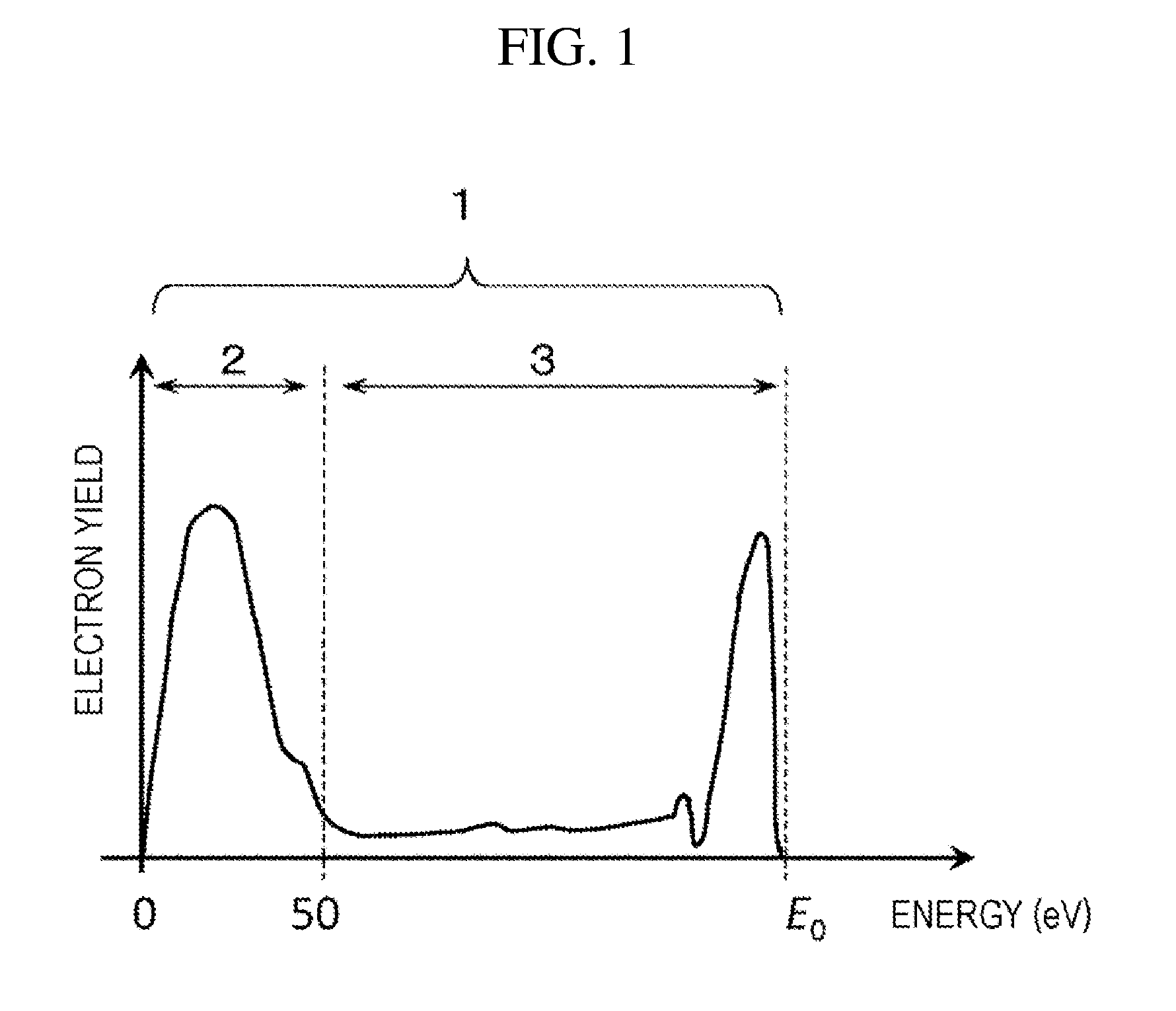
TECHNICAL FIELD[0001]The present invention relates to a scanning electron microscope that detects a signal electron having passed through an objective lens.BACKGROUND ART[0002]There is a widely known Scanning Electron Microscope (SEM). To acquire a two-dimensional image of a scanning region on the surface of a sample, this SEM detects a signal electron generated when the sample is scanned by an irradiation electron beam converged on the sample and displays the signal strength at each irradiation position in synchronization with a scanning signal of the irradiation electron beam.[0003]In an ordinary SEM, the chromatic aberration increases in a low-acceleration region, and a high resolution cannot be achieved. To reduce the chromatic aberration, the deceleration method is effective. By the deceleration method, high-speed passage is made through an objective lens, and irradiation is performed by decelerating the irradiation electron beam directly in front of the sample. Application of ...

Claims


Application Information

Patent Timeline
IPC IPC(8): H01J37/26H01J37/244H01J37/28
CPCH01J37/265H01J37/28H01J37/244H01J2237/0475H01J2237/2448H01J2237/1534H01J2237/103H01J2237/24475
Inventor AGEMURA, TOSHIHIDEMORISHITA, HIDEO
Owner HITACHI HIGH-TECH CORP
Learn More