Organic semiconductor composition, organic thin film transistor, electronic paper and display device

a technology of organic thin film transistors and semiconductor compositions, applied in the direction of non-metal conductors, conductors, thermoelectric devices, etc., can solve the problems that the insulation reliability between source electrodes and drain electrodes do not meet the current required level, so as to improve the insulation reliability reduce the mobility of organic thin film transistors

Inactive Publication Date: 2016-06-02
FUJIFILM CORP
View PDF3 Cites 1 Cited by
  • Summary
  • Abstract
  • Description
  • Claims
  • Application Information

AI Technical Summary

Benefits of technology

[0023]According to the present invention, it is possible to provide an organic semiconductor composition, which improves the insulation reliability of an organic thin film transis

Problems solved by technology

As a result, it was revealed that either or both of the mobility of the organic thin film transistor and the in

Method used


Image

  • Organic semiconductor composition, organic thin film transistor, electronic paper and display device
  • Organic semiconductor composition, organic thin film transistor, electronic paper and display device
  • Organic semiconductor composition, organic thin film transistor, electronic paper and display device

Examples


example 1

Preparation of Organic Semiconductor Composition

[0147]The organic semiconductor material a-1 and the anti-migration agent b-1 were dissolved in toluene (organic semiconductor material a-1 / anti-migration agent b-1=100 parts by mass / 50 parts by mass (w / w), organic semiconductor concentration: 1.5% by mass), thereby preparing an organic semiconductor composition. The obtained organic semiconductor composition was named a composition 1.

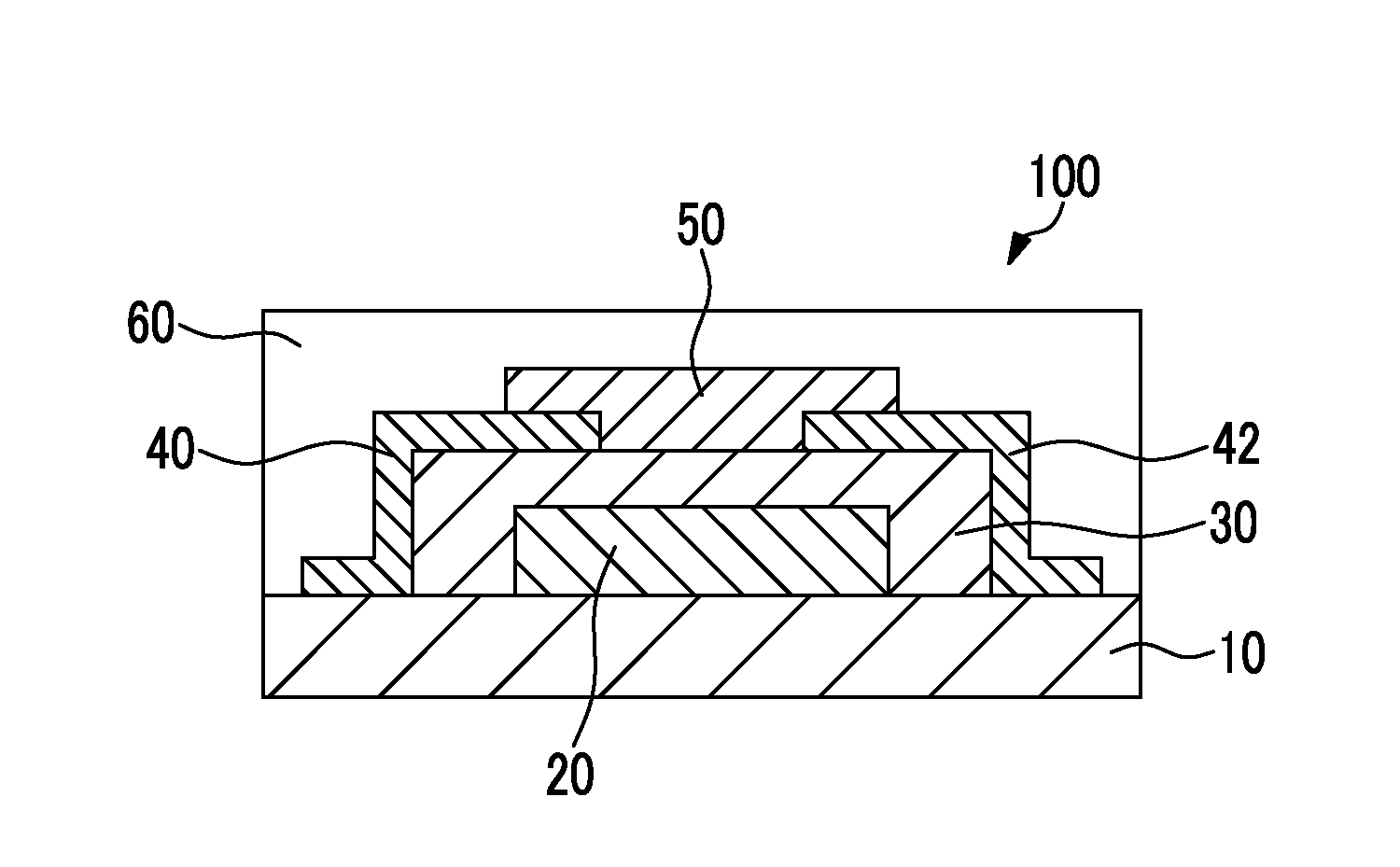
[0148](Preparation of Organic Thin Film Transistor (Element Preparation Method 1))

[0149]Al which will become a gate electrode was vapor-deposited (thickness: 50 nm) onto a glass substrate (Eagle XG: manufactured by Corning Incorporated). The Al layer was spin-coated with a composition for forming a gate insulating film (a propylene glycol monomethyl ether acetate (PGMEA) solution (solution concentration: 2% by mass) of polyvinylphenol / melamine=1 part by mass / i part by mass (w / w)), and the composition was baked for 60 minutes at a temperature of 150° C., t...
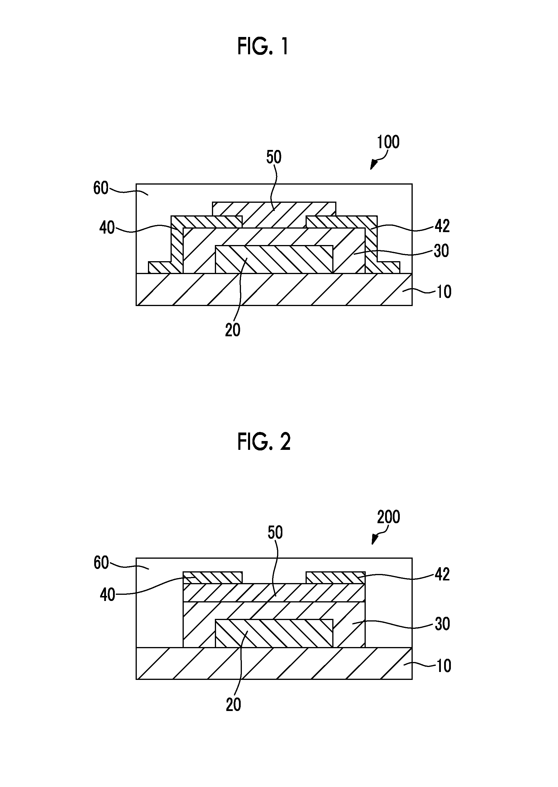
example 2

[0164]An organic thin film transistor was prepared according to the same procedure as in Example 1, except that the following element preparation method 2 was performed instead of the element preparation method 1. Furthermore, according to the same procedure as in Example 1, various evaluations were performed. The results are summarized in Table 1.

[0165](Preparation of Organic Thin Film Transistor (Element Preparation Method 2))

[0166]Al which will become a gate electrode was vapor-deposited (film thickness: 50 nm) onto a glass substrate (Eagle XG: manufactured by Corning Incorporated). The Al layer was spin-coated with a composition for forming a gate insulating film (a PGMEA solution (solution concentration: 2% by mass) of polyvinylphenol / melamine=1 part by mass / I part by mass (w / w)), and the composition was baked for 60 minutes at a temperature of 150° C., thereby forming an insulating film having a film thickness of 400 nm. The insulating film was spin-coated with the prepared co...


PUM

PropertyMeasurementUnit
Compositionaaaaaaaaaa
Molecular weightaaaaaaaaaa
Semiconductor propertiesaaaaaaaaaa

Abstract

The present invention provides an organic semiconductor composition, which improves the insulation reliability of an organic thin film transistor without greatly reducing the mobility of the organic thin film transistor, and an organic thin film transistor, electronic paper, and a display device which are prepared by using the organic semiconductor composition. The organic semiconductor composition of the present invention contains an organic semiconductor material and an anti-migration agent containing at least either a compound X, which contains at least two or more groups selected from the group consisting of a group represented by Formula (A) and a group represented by Formula (B), or a compound Y which is represented by Formula (C).

Description

[0001]This application is a Continuation of PCT International Application No. PCT / JP2014 / 067906 filed on Jul. 4, 2014, which claims priority under 35 U.S.C. §119(a) to Japanese Patent Application No. 2013-158767 filed on Jul. 31, 2013. Each of the above application(s) is hereby expressly incorporated by reference, in its entirety, into the present application.BACKGROUND OF THE INVENTION[0002]1. Field of the Invention[0003]The present invention relates to an organic semiconductor composition, an organic thin film transistor, electronic paper, and a display device.[0004]2. Description of the Related Art[0005]In apparatuses using a logic circuit such as a thin film transistor (TFT), RF tag (RFID), or memory used in a liquid crystal display or an organic EL display, an organic semiconductor device having an organic semiconductor film (organic semiconductor layer) composed of an organic semiconductor material is used, because the use of the organic semiconductor device makes it possible ...

Claims


Application Information

Patent Timeline
IPC IPC(8): H01L51/00
CPCH01L51/0094H01L51/0036H01L51/0067H01L51/0558H01L51/0055H01L51/0074H01L51/005H01B1/121H10K10/484C08K5/00H10K85/40H10K85/60H10K85/113H10K85/654H10K85/623H10K85/6576
Inventor MATSUSHITA, YASUAKIMATSUMURA, TOKIHIKO
Owner FUJIFILM CORP
Why Eureka
Try Eureka